
In the past, I used to build project prototypes through breadboards and perfboards. However, the emergence of affordable PCB manufactures have allowed me to go away from my old ways of prototyping. In this article, I will share how I created the PCB board for my SIMPic development board through JLCPCB.
Just like other PCB services, JLCPCB requires gerber files. I used Eagle to create the schematic and subsequently, the PCB layout for the SIMPic board.
Generating Gerber Files
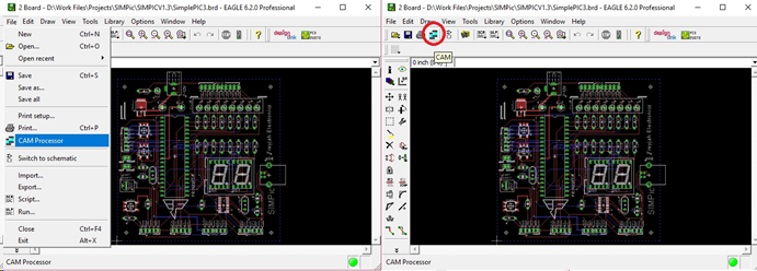
In Eagle’s board view, select CAM Processor from File > Cam Processor or click the CAM icon on the upper left:
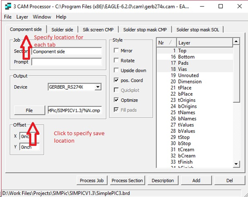
In the CAM processor window, open a job via File > Open > Job. Select gerb274x.cam. Multiple tabs should now be visible. These tabs correspond to different parts of the PCB. You’ll need to specify the location of the output files for each tab by clicking the File button as shown:
After going through all the tabs and specifying their save locations, click Process Job:
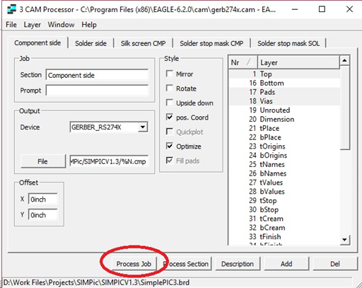
The program should now create files on the location you specify with the following extensions: .cmp, .gpi, .plc, .sol, .stc, .sts.
Gerber Files for Drilling
If holes for screws are needed, you need a separate job. On the same CAM processor window, select File > Open > Jobs again and choose, excellon.cam. The program may ask you to save the previous job.
A new CAM processor window should appear:
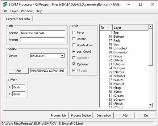
As before, specify the location by clicking the File button and then click Process Job. The .drd and .dri files should now be created on the location specified if successful.
Here’s all the files needed by JLCPCB:
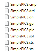
I placed them inside a folder and then zipped that folder.
Submitting the Gerber Files
To submit the gerber files to JLCPCB, create or login to your account and go to the Calculate page:
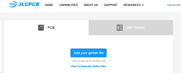
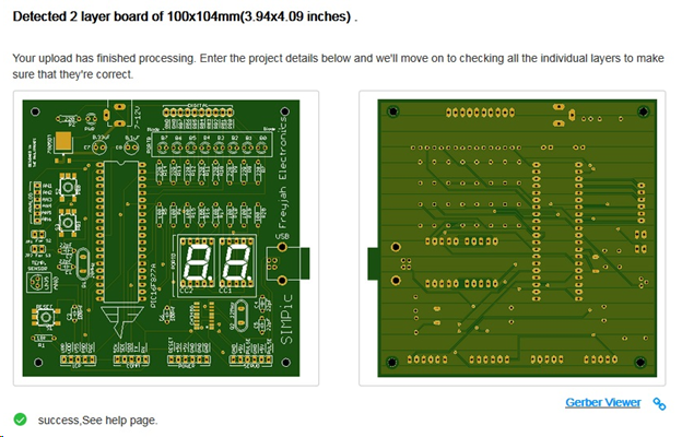
Click the “Add your gerber file” button to upload the zipped gerber files folder. If all the required files are there, you should be able to view the PCB layout:

Here, JLCPCB also states my board dimensions. Note that you can’t avail of the $2 PCB promo if your board exceeds 100 mm x 100 mm.
On the bottom part is the area where I can specify other parameters for my board:
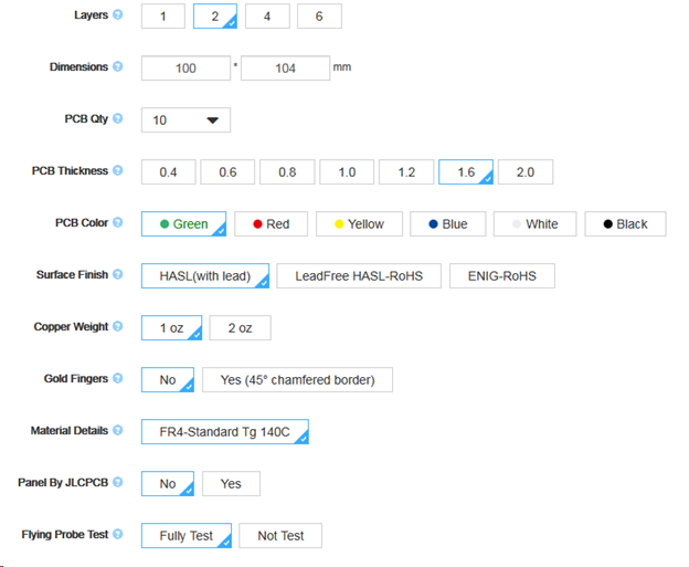
Note that additional charges may be added for different parameters.
Clicking the Gerber Viewer link gives a better view of my board:
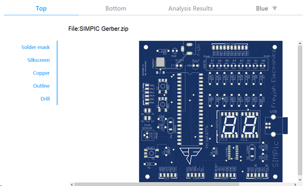
Here I can hide or show the different layers of my board as prescribed in the gerber files. I can also select which color looks good on my board. Blue looks cool!
Go back to the Calculate page and checkout to start the order process. To give you an idea, my board costs $40.96 including shipping via DHL. The price is due to my board exceeding 100 x 100 mm and using blue paint instead of the default green. If you’re board is within the mentioned size limits and paint color, $19.50 including shipping.
Finished Product
JLCPCB took only two days to finish and deliver my board. Here is now the finished product:
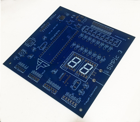
It looks awesome!