
Vias are very common when designing PCBs. I myself have used PCB via even before fully understanding them. In this article, I will be sharing the different types of vias and how they are actually used in PCB design.
What Is a Via?
In general terms, a via connects one PCB layer to another. Vias may join traces, pads and other conductive elements on a PCB through a copper cylinder placed inside holes. These holes pass through the affected layers on the board.
PCB Vias need a certain volume of copper on a layer to ensure that the layers are really connected. In this regard, a via pad, which is a circle of copper, is connected to the endpoint of traces, specifically narrow ones.
An antipad is an area of the via without copper. This is necessary in order to insulate the via pad from the other conductive materials nearby.
A via connecting two PCB traces is shown below:

Creating Vias
DIY hobbyists typically don’t use vias in their PCBs. Actually, vias are only possible if you acquire the services of PCB manufacturers. A cross-section of a via is shown below:

First, holes are drilled through the PCB where the via is supposed to go. Then, a special chemical is poured inside that hole which dissolves the epoxy on the internal layers. Dissolving the epoxy between layers is important to expose the interior copper pads. After that, copper is applied to the hole via electroplating process.
Using Vias in PCB Design
As mentioned, vias create a connection between layers in a multiple-layer PCB. But aside from that, vias also allow thermal energy from one layer to dissipate into other layers of the board. This will help reduce the thermal energy dissipated by an integrated circuit, for example. The thermal pads of the IC is usually connected to vias to the other layers.
A QFN IC package shown below has 65 vias connected to its thermal pad:

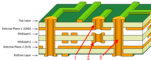
Kinds of Vias
As far as basic vias are concerned, there are three distinct types:
- Blind vias
- Buried vias
- Through vias
A blind via connectes an exterior (visible) layer to an interior (invisible) layer. A buried via connects two interior layers. Lastly, a through via connects two exterior layers. The three types of vias are illustrated above.
Naturally, you can’t use blind or buried vias if you have a two-layer PCB. Blind or buried vias are used in three or more layered PCBs and are generally at an additional cost. Buried vias are seldom used unless necessary because they are very hard to troubleshoot.
Again, the choice of via would depend on the number of layers of your PCB and your budget.
Choosing the Right Via Size
Choosing the right size of your via actually depends on the capabilities of your PCB manufacturer! JLCPCB, for example, is not particular with the size of your holes but other companies do!
Take note that typical drills won’t go lower than 12 mils in diameter while annular rings’ (circular copper) minimum size is around 6 mil.


thanks for us