
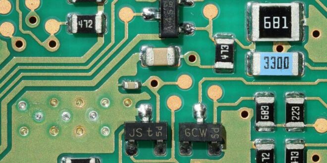
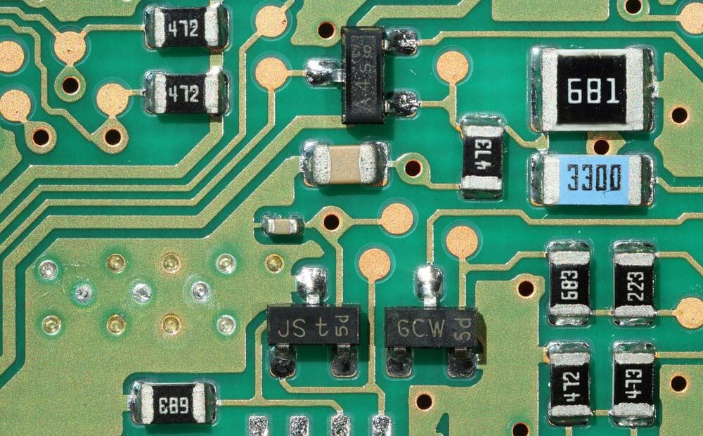
Printed Circuit Boards or PCBs are essential elements in the electronic world. They are used in more straightforward gadgets such as toys to complex devices such as military equipment.
Nevertheless, standard PCBs usually are used in low-power and low-voltage devices. This is to help them work properly. But what kind of PCB is used on devices that require more power and voltage?
In this article, you will learn everything you need to know when it comes to heavy copper PCB. You will learn what heavy copper PCB is, the benefits of heavy copper PCB, the manufacturing process of heavy copper PCB, and much more.
What is heavy copper PCB?
A heavy copper PCB is a printed circuit board with a copper thickness of 3oz per sq. ft. But what makes a circuit board categorized as a heavy copper PCB is the thickness of its plating.
Copper thickness is improved by producing heavy copper PCB through plated holes and sidewalls. For example, if a PCB has two ounces of copper per sq. ft. thickness, that is a standard PCB.
But if the PCB has more than 3oz of copper, it is classified as heavy copper PCB. Nevertheless, a heavy copper PCB is different from an extreme copper PCB. An extreme copper PCB features 20oz to 200oz per sq. ft.
With the heavy copper PCB, the thickness helps the board conduct more current. The boards have more substantial mechanical power in the connector sites than the standard PCBs.
The benefits of heavy copper PCB
Heavy copper PCB comes with many benefits. Due to its unique features, it has become a perfect option for high-end applications. Here are the main benefits of heavy copper PCB.
1. Good thermal distribution
Due to their copper-plated vias, heavy copper PCBs provide good thermal distribution. Hence, they are used in applications that require high frequency and high speed. The PCB can be used in harsh temperatures.
2. Great mechanical strength
Another benefit of heavy copper PCB is its excellent mechanical strength. This makes it more durable and robust.
3. Excellent conductor
A heavy copper PCB is an excellent conductor. Hence, the PCB is used to produce various electronics due to this benefit. It is possible to link several boards together, and they can quickly transfer current.
4. Have an excellent dissipation factor
Heavy copper PCBs are perfect for significant elements with a high loss of power. This is because they have an excellent dissipation factor. They prevent overheating from happening in electrical systems.
Difference between standard PCB and heavy copper PCB
1. Standard PCBs are quickly produced with copper etching and plating processes. The boards are plated to increase copper thickness to traces and planes. Also, the amount of copper used in standard PCBs is 1oz.
On the other hand, there are different manufacturing methods for heavy copper PCBs and the amount of copper used is more than 3oz.
2. With the standard printed circuit boards, cnc cutting, copper etching and plating methods are utilized. But heavy copper PCBs are obtained through various etching and step plating methods.
3. Standard PCBs perform lighter duties while heavy copper printed circuit boards perform heavy tasks. Also, the standard ones conduct a lower current while the heavy PCBs conduct a heavy current.
The manufacturing process of heavy copper PCB
When it comes to manufacturing heavy copper PCBs, there are several steps to be considered. However, plating or etching is usually used.
Plating or etching aims to add copper thickness to plated holes or sidewalls. However, heavy copper PCBs require unique etching and plating methods. This is to make sure there is an extra thickness of copper.
When standard etching techniques are used, the manufacture of heavy copper PCB is not complete. The traditional etching techniques only produce over-etched edge lines that are not even.
Throughout the manufacturing process of heavy copper PCBs, they are electroplated. This helps in thickening the walls on the PCB.
Nevertheless, the manufacturing of heavy copper has its limitations. For instance, the etching process increases the cost and requires a significant amount of copper to be removed. Also, the heavy copper traces make the surface uneven.
Methods for manufacturing heavy copper PCBs
Blue Bar Method
This is a method that is used to create automobile PCBs. It involves inserting thick copper bars onto PCBs to move the extra current. Since only a few lines are required to transmit more current in a high-power circuit. The method helps save cost and money since it reduces the weight of the PCB.
Embedded Copper Method
With this method, a thick copper PCB and a heavy copper and a flat surface are combined to create the prepreg resin. The thickness of the resin determines the thickness of the heavy copper used.
Heavy Copper PCB Capabilities
Here are the key capabilities that should be available on heavy copper PCB
- The board size of 457mm * 610mm maximum and 6mm * a 6mm minimum is needed.
- Copper thickness should be more than 3oz per sq. ft.
- Blue, green, red, black, white, yellow, or purple solder masks are suggested.
- The silkscreen color should either be yellow, white, or black.
Applications of heavy copper PCB
Heavy copper PCBs come with numerous benefits over standard PCBs. In addition, they offer outstanding features making them perfect for specific applications.
For instance, heavy copper PCBs are ideal for defense and military applications, medical devices, and many other areas. Hence, the demand for heavy copper PCBs is continuously increasing.
Some of the applications of heavy copper PCBs are:
- Solar power converters
- Rail traction systems
- Nuclear power industries
- Automotive industries
- UPS systems
- Protective relays
- Torque controls
- Safety and signal systems
- Welding equipment
- Power line motors
- Military equipment
Conclusion
Due to their outstanding features and benefits, heavy copper PCBs are impressive and can meet your electrical needs. They can carry high currents and meet the needs of various applications.
They are widely used in various fields since they provide multiple remarkable features. However, it is essential to learn the benefits and limitations of the board before designing.


")


