
Using the Raspberry Pi Pico is convenient, but as you level up your project, you’ll find that it is much better to create your own PCB that satisfies your design requirements.
If you have designed PCB boards for STM32 microcontrollers before, then you’ll find that it is not much different from designing for an RP2040 microcontroller. Nevertheless, THERE IS a difference and this article will outline all the things you need to consider prior to submitting your PCB layout for mass production.
Comparison with Other ARM Microcontrollers
The STM32F103R, commonly featured on this website, is a close comparison to the RP2040. But in terms of PCB layout, here are the areas where the RP2040 stands out:
- QFN Package: Unlike the STM32F103R, the RP2040 only comes in a QFN package which means soldering is a nightmare for hobbyists relying on soldering iron. Moreover, the chip itself is only 7.75 x 7.75 mm and the PCB pad width and spacing are 0.20 mm. Make sure your choice of PCB company is able to handle such small footprints.
- No. of Cores: The RP2040 has twice the number of cores as the STM32F103R. Normally, this results in higher power consumption. In PCB design, trace width must be adjusted according to power -- higher power means wider trace width.
- External SPI Flash: Another peculiar thing about the RP2040 is that it requires an external SPI flash component. This component is very important as it is the primary non-volatile storage for the microcontroller. And so the PCB traces must be optimized to ensure the highest data speed possible while minimizing the effects of noise.
Power Considerations
We have been designing boards for microcontroller systems and it’s common to have two levels of voltage supplies. But the RP2040 is unique in the sense that it requires 3.3V for peripherals but only 1.1V for its digital core (DVDD).
The RP2040 datasheet suggests that DVDD can be wired directly to VREG_VOUT, which also produces 1.1 V. VREG_VOUT is an output from an internal LDO -- experience has thought us that an internal LDO’s efficiency comes and goes with a core’s workload. That is, when the RP2040 is pumping up its computational powers, the LDO may swing from its intended output. Hence, an external 1.1V source is much more recommended.
Decoupling capacitors are also important components in RP2040’s power supply. It is highly recommended that such capacitors (100 nF per power pin) are as close to power pins as possible. This is because decoupling capacitors both filter out power supply noise and become instant charge supply.
BTW, if you opt to use the internal LDO, it requires its own 1uF decoupling capacitors and must be physically small to reduce the effects of ESR.
Crystal Oscillator
To be clear, the RP2040 doesn’t require an external crystal oscillator. Nevertheless, the Raspberry Pi foundation recommends using one because it is much more stable than the RP2040’s internal oscillator.
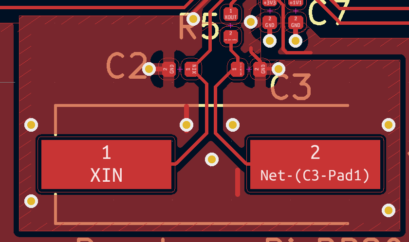
PCB design is critical to an external oscillator, like in other microcontrollers. First and foremost, the load capacitors must be very close to the crystal. The farther the load capacitors, the higher the parasitic capacitance introduced. This added capacitance, of course, changes the overall load capacitance required by the RP2040 for its oscillator.
Since this is a signal generating pin, keep the XIN and XOUT pins far away from other (high-speed) signal pins to avoid crosstalk and interference.
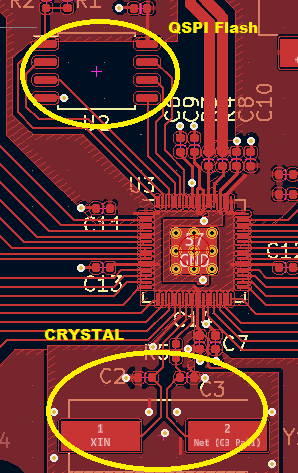
Here’s an example layout of an external crystal with its load capacitors:
This is on the opposite side, far away from the QSPI flash chip:
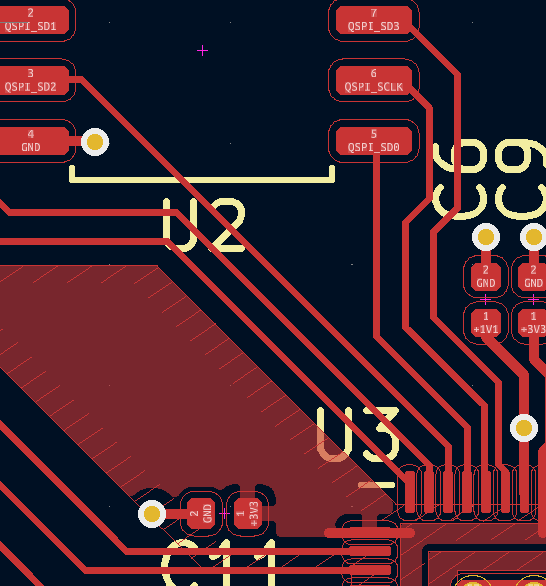
SPI Flash Chip
The Quad SPI flash chip acts like the Raspberry Pi’s sd card -- without it, the RP2040 will not boot at all. The RP2040 supports up to 16 MB of flash storage. This is the maximum memory size selectable so you can select flash chips lower than this. Although it is recommended to go with a QSPI flash that is comparable to Winbond’s W25Q128JVS. To be safe, just stick with Winbond’s W25Q series.
As for PCB design, the RP2040 QSPI pins must be wired as close to the external QSPI flash IC as possible to avoid crosstalk. The trace length must not exceed 20 mm while a trace width of 0.15 mm should be ok.
Other things to consider:
- For non-W25Q flash chips, there must be a pull-up resistor from the QSPI_SS pin to the board’s 3.3V line.
- Another resistor (1k) is in series with the QSPI_SS and USB_BOOT. This is required for both W25Q and non-W25Q flash chips
- When doing the PCB layout, both above-mentioned resistors must be close to the flash chip. Longer traces will affect the signal.
- Ground planes are always a good idea; create one that readily connects the ground pin of the QSPI flash.
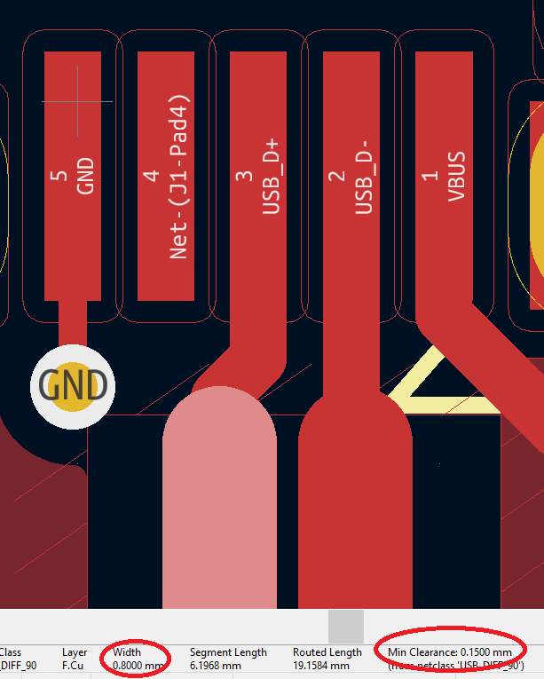
USB Trace
For USB traces, a trace width of 0.8 mm with a spacing of 0.15 mm for a 1 mm board is recommended. If this is not possible, use a microstrip impedance calculator to achieve the correct dimensions for an impedance of 90 ohms.
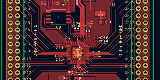
GPIO Headers
Then there are the GPIO headers which are a pair of 2x18 2.54 mm headers to which the rest of the RP2040’s IO connects. On the sample PCB layout by the Raspberry Pi foundation, the outer rows are always ground pins while the inner pins are the IOs:
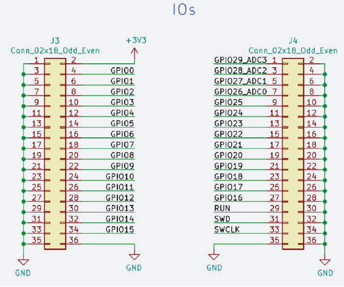
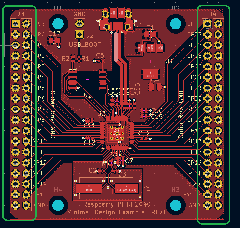
This scheme is not required, but I personally found it convenient when designing the PCB. It actually has the advantage of minimizing electromagnetic interference because the return currents now take a shorter path.
In summary, for a basic PCB design featuring the RP2040 microcontroller:
- Prepare to use as many SMD components as possible, with RP2040 itself being a tiny QFN
- Be careful in designing the layout for the QSPI flash chip: make signal traces shorter than 20 mm with a width of 0.15 mm
- Keep external crystal and its traces far away from other high-speed traces like the QSPI; also keep the load capacitors close to the crystal
- USB traces must be 0.8 mm in width and 0.15 mm in spacing
- For the headers, keep one side all connected to the ground to minimize electromagnetic interference
- Use ground planes as much as possible!
With these PCB design tips in mind, make sure to choose a capable PCB manufacturer. PCBgogo has no problems building PCBs with trace width as low as 0.07 mm or thickness of as low as 0.4 mm.
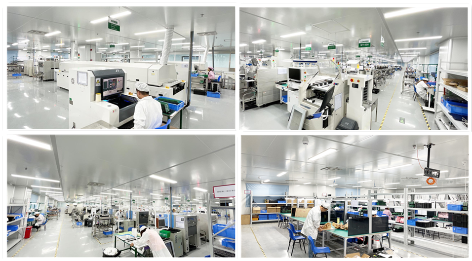
Afraid of soldering the tiny QFN package and other SMD components yourself? PCBgogo also offers precise component placement and turnkey PCB assembly services with them sourcing all the needed components!
PCBgogo also maintains good communication with its customers for special requests. This ensures that your RP2040 PCB is done according to specifications.


