Flexible PCB assembly looks simple until the first build goes wrong.
A flex circuit is thin, light, and easy to bend, but those same features make it harder to assemble consistently. The circuit can shift during printing, wrinkle during handling, absorb moisture, expand under heat, or crack near a bend if the layout and assembly process are not planned together.
This is why flexible PCB assembly should not be treated as standard SMT on a thinner board. The process has to account for both electronics and mechanics. A solder joint may pass inspection on a flat fixture, but fail later when the circuit is folded into an enclosure, pulled by a connector, or bent during installation.
For products such as wearables, camera modules, medical sensors, battery packs, folded displays, handheld devices, and industrial controls, the flex circuit is often part of the mechanical structure. That means the assembly process needs to control more than component placement. It also needs to control support, bending areas, stiffeners, connector loads, inspection access, and final handling.
Flexible PCB Assembly Starts Before Production
The most important part of flexible PCB assembly happens before the board reaches the SMT line.
A proper review should include the FPC fabrication data, BOM, pick-and-place file, assembly drawing, polarity notes, test plan, stiffener locations, bend areas, coverlay openings, connector locations, and final installation posture.
This review is not just a formality. Many FPC assembly problems start because the electrical design is finished before anyone checks how the circuit will be assembled or used.
For example, components should generally stay out of active bend areas. Vias, plated holes, pad edges, copper width transitions, coverlay openings, and stiffener edges also need attention because they can concentrate stress. A small layout detail that looks harmless on screen can become the exact place where copper cracks after repeated bending.
Before production, the team should be able to answer three basic questions:
- Which areas must stay flat during printing, placement, and reflow?
- Which areas will bend, pull, fold, plug, or carry strain after assembly?
- Which solder joints or nets cannot be checked by visual inspection alone?
If these questions are not answered early, the SMT line may still build the board, but the product may not be reliable.
Data Package and DFM Review
The first real process step is checking that all files describe the same build.
The fabrication files, BOM, stencil data, centroid file, assembly drawing, test requirements, and revision history must match. This sounds basic, but mismatched revisions are one of the easiest ways to create avoidable assembly errors.
A good DFM review should look for missing fiducials, unsupported fine-pitch parts, unclear polarity marks, missing DNP instructions, insufficient connector support, poor access for inspection, and components placed too close to flexing areas.
Substitutions also need extra care on FPC assemblies. A connector with the same pin count but a slightly different housing shape, solder tail geometry, insertion force, or height can change the mechanical behavior of the whole assembly. In rigid PCB assembly, that kind of change may be manageable. On a flex circuit, it can create stress in the wrong place.
When a project uses outside PCB assembly services, the release package should make these details clear before the quote is finalized, not after the first article build has already started.
Incoming FPC and Component Control
Incoming inspection matters more for FPCs than many teams expect.
The flex circuit should be checked for surface finish condition, contamination, coverlay registration, pad exposure, stiffener placement, panel flatness, edge damage, lot identification, and packaging condition. Even minor bending, dents, or contamination can affect solder paste printing and placement accuracy.
Component handling is also important. Fine-pitch connectors, bottom-terminated packages, LEDs, sensors, and moisture-sensitive devices may need controlled storage and handling. If solderability testing or special inspection is required, it should be defined in the purchasing documents or quality plan.
Do not assume that a generic incoming inspection process covers every flex-related risk. Flexible assemblies bring mechanical risks that may not appear on a normal rigid board checklist.
Carrier and Fixture Strategy
The first practical challenge is simple: a flexible circuit needs to behave like a stable panel long enough to be assembled.
That usually requires some form of support. Depending on the design, this may include a temporary carrier, vacuum fixture, edge frame, tooling holes, local hold-downs, high-temperature tape, or removable support.
The carrier is not just a production aid. It affects paste print quality, component placement accuracy, reflow heating, inspection access, and removal risk.
A good carrier should support the areas that must stay flat without pressing on pads, bend zones, coverlay edges, or components. It should also survive the thermal process without shifting the circuit or creating new stress.
One common mistake is profiling reflow without the real carrier. That can give a false picture of the soldering process. The carrier adds thermal mass and can change the heating rate across the assembly. If the carrier is used in production, it should be included in the reflow profile validation.
Stencil Design and Solder Paste Printing
Stencil design for flexible PCB assembly should not be a direct copy of the copper pads.
The team needs to consider aperture shape, stencil thickness, fine-pitch bridging risk, QFN thermal pad behavior, connector solder volume, local paste reduction, and the flatness of the supported FPC panel.
Solder paste inspection is especially useful during setup because a flex circuit may not sit as flat as a rigid board. Local deflection can cause uneven paste deposits. That may lead to bridging, insufficient solder, tombstoning, or weak joints after reflow.
It is usually cheaper to control paste printing early than to discover solder defects after reflow. For a flex build, that early setup time is well spent.
SMT Placement on a Flexible Substrate
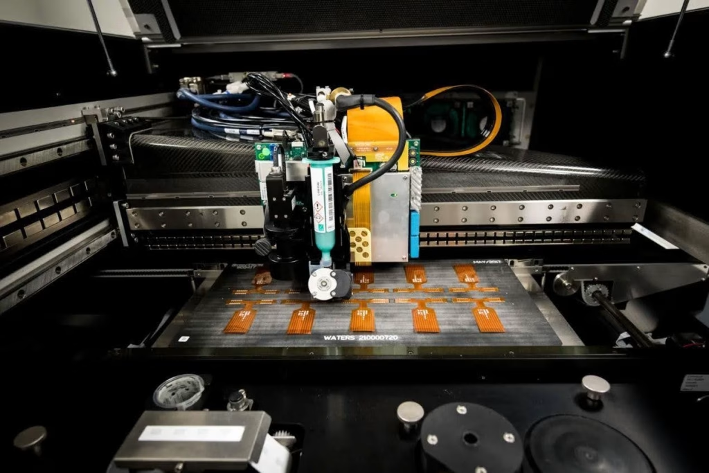
Placement accuracy depends on the stability of the panel.
A flexible circuit can shift slightly under nozzle pressure or move if the fixture does not hold it evenly. This is especially important for small passives, fine-pitch connectors, QFNs, BGAs, and lightweight sensors.
The placement program may need adjusted support height, board thickness settings, nozzle selection, placement force, fiducial strategy, and placement sequence. Even a small amount of movement can cause skew or marginal solder joints.
First article inspection should check not only component position, but also handling damage. A slight crease in the wrong area may not matter visually, but it can become a reliability issue once the circuit is installed and bent.
Reflow Profiling With the Real Build
Reflow is another place where flex assemblies can be underestimated.
The FPC material, carrier, stiffeners, connectors, adhesives, and larger components all affect how the assembly heats. A profile copied from a rigid PCB job may not work for the actual flex build.
The right approach is to profile the real panel on the real carrier. Thermocouples should be placed in meaningful areas, such as fine-pitch connector zones, stiffener edges, slow-heating regions, board edges, and temperature-sensitive components.
The final profile should stay within the solder paste supplier’s process guidance, component limits, and material constraints of the FPC construction.
If the assembly requires double-sided reflow, hand soldering, connector rework, heat staking, adhesive bonding, or shield film lamination, those heating steps should be considered as part of the total thermal history. They should not be treated as separate events with no effect on the flex.
Stiffeners, Connectors, and Secondary Operations
Stiffeners are often used around connectors, solder tabs, keypad areas, screw locations, and interface zones. They may be made from polyimide, FR-4, stainless steel, or other materials depending on the required thickness, rigidity, temperature exposure, and adhesive method.
A stiffener can solve one problem and create another if it is placed poorly. The edge of a stiffener can shift stress into copper traces, coverlay openings, or solder joints. For connector areas, the team should consider insertion force, cable pull direction, latch geometry, adhesive area, and housing support.
Secondary operations may include hand soldering, selective soldering, conductive adhesive, pressure-sensitive adhesive, shield film lamination, conformal coating, or forming. Each step should have process limits, inspection criteria, and rework rules.
This is one reason it is often safer to work with a flexible PCB manufacturer that understands both fabrication and assembly. A flex build is not just about getting the board made. It is about controlling how the circuit behaves after components, stiffeners, connectors, and mechanical loads are added.
Cleaning, Rework, and Handling
Cleaning depends on flux chemistry, product environment, insulation requirements, coating needs, and customer specifications.
A no-clean process does not automatically mean residues are acceptable in every product. High-impedance circuits, medical electronics, sensor inputs, humid environments, and long-life industrial equipment may need a closer look at residue risk.
Rework also needs stricter control on flex assemblies. Hot air, soldering irons, connector replacement, stiffener repair, and local heating can damage coverlay, adhesive, copper, or pads.
The production plan should define which parts may be reworked, how many attempts are allowed, what temperature controls are required, and what inspection or testing must follow rework. Without those limits, rework can easily create hidden damage.
Handling should be controlled from start to finish. Flex circuits should not be bent casually, stacked under weight, pulled by connectors, or packed in a way that creates stress at stiffener edges or solder joints.
Inspection and Test
AOI is useful for visible defects such as missing parts, polarity errors, skew, tombstoning, bridging, and many solder joint issues. X-ray is better for hidden joints, including BGAs, QFNs, bottom-terminated parts, and some voiding concerns.
Manual microscope inspection is still important around connector pins, flex edges, coverlay openings, stiffener transitions, and areas where handling damage is suspected.
Electrical testing should match the product’s real failure risks. A test plan may include continuity, opens and shorts, ICT, flying probe, functional test, connector verification, insulation checks, or resistance monitoring while the flex is held in a defined bend position.
A static electrical pass at room temperature does not prove the assembly will survive installation or repeated movement. If the product has dynamic flexing, the qualification plan should define bend radius, cycle count, resistance change limits, inspection method, and acceptance criteria based on the actual use case.
Process Records and Final Packaging
For production FPC assemblies, process records are part of the product.
Useful records may include DFM notes, carrier setup information, first article inspection results, SPI data, reflow profiles, AOI records, X-ray images, functional test logs, rework history, and lot traceability.
These records help the engineering team separate design issues from process drift if a failure appears later.
Packaging is also part of the process. The final packaging should prevent creasing, uncontrolled bending, connector damage, contamination, and ESD events. If the flex assembly has a formed shape, the packaging should preserve that shape without creating stress at stiffener edges or solder joints.
Common Failure Modes in Flexible PCB Assembly
Copper cracking is one of the most common flex-circuit failures. It often appears near bend zones, stiffener edges, via barrels, copper width transitions, pad edges, or places where the circuit is folded tighter than expected.
Solder joint cracking usually appears near connectors, large components, board edges, and areas exposed to pull or twist. Adding more solder is not always a fix. In some cases, too much solder changes the stress shape and creates new problems.
Coverlay cracking and pad lifting may come from window geometry, heat exposure, rework, or mechanical stress. These issues are often seen near bend transitions or areas that were heated repeatedly during repair.
Connector failures can be misleading because the solder joints may look fine after reflow. Problems often show up later during cable insertion, latch engagement, pull testing, or final housing assembly.
Shielding can also change the mechanical behavior of the flex. Shield films, ground foils, conductive adhesives, and copper shields may help with EMI control, but they add thickness and stiffness. On a flex assembly, EMI shielding should be reviewed as both an electrical feature and a mechanical feature.
How IPC Standards Fit In
IPC standards help define design, fabrication, soldering, and acceptability expectations. They should not be used as a vague quality label.
For flexible and rigid-flex design, IPC-2223 is commonly referenced. For flexible printed board performance and qualification, IPC-6013 is commonly used. Soldered assembly requirements may involve J-STD-001, while assembled board acceptability is commonly evaluated against IPC-A-610. Material requirements may route to IPC-4204, and solderability testing may involve J-STD-003 when required.
The key is to define the correct standard, revision, class, product type, and customer exceptions in the project documentation. Saying a build “meets IPC” is not enough unless the team knows which document, which class, and which inspection criteria apply.
Questions to Close Before Production
Before a flexible PCB assembly moves into production, it is worth closing these questions:
- Is the flex use case static, flex-to-install, or dynamic?
- Are components, vias, solder joints, and stiffener edges kept out of high-stress bend regions?
- Has the carrier been validated through printing, placement, reflow, inspection, and removal?
- Was the stencil reviewed for FPC flatness, fine-pitch parts, and local paste volume?
- Was the reflow profile measured on the actual production carrier?
- Which hidden solder joints require X-ray or another nonvisual inspection method?
- Does the test plan reflect the final installation posture and bend condition?
- Are rework limits and retest rules documented?
- Are IPC standards, customer requirements, and exceptions clearly listed?
If these questions are still open, the build may work at prototype level, but production risk remains high.
Conclusion
Flexible PCB assembly is not easy, and it is not simply a thinner version of rigid PCB assembly.
Thin materials, bend areas, stiffener edges, connector loads, thermal exposure, limited inspection access, and handling sensitivity can all create failures if they are not reviewed early. A reliable process depends on DFM review, carrier support, stencil design, placement stability, reflow profiling, reinforcement strategy, inspection, electrical test, bend validation, and controlled handling.
The best results come when the flex circuit is treated as an electromechanical product before the design is frozen. When bend areas, connector loads, solder joint access, IPC requirements, and test evidence are defined early, the assembly process becomes a practical quality plan instead of a generic process list.
FAQ
What makes flexible PCB assembly different from rigid PCB assembly?
The main difference is mechanical behavior. A rigid PCB usually stays flat during printing, placement, reflow, and test. A flexible PCB needs controlled support and handling because it may bend, move, or deform during production and later use.
Do all flexible PCBs need a carrier during SMT assembly?
Not every flex circuit needs a dedicated carrier, but many SMT flex assemblies need some form of support. The need depends on FPC thickness, panel size, component weight, placement accuracy, reflow exposure, and equipment clamping.
Can components be placed in a bend area?
In most cases, components, solder joints, vias, and stiffener edges should stay out of active bend regions. Some special designs may allow controlled bending near components, but that should be validated by the design, fabrication, and assembly teams.
Can AOI replace X-ray inspection?
No. AOI is useful for visible defects, while X-ray is used for hidden solder joints such as BGAs, QFNs, and bottom-terminated components. The inspection method should match the package type and failure risk.
Which IPC standards are relevant to flexible PCB assembly?
Common references include IPC-2223, IPC-6013, J-STD-001, IPC-A-610, IPC-4204, and J-STD-003. The exact standard, revision, class, and customer exceptions should be defined in the project documents.
How do you know an FPC assembly process is ready for production?
The process is ready when DFM issues are closed, the carrier and stencil are validated, the reflow profile is documented, inspection and test coverage match the product risks, bend-related concerns are reviewed, and rework rules are defined.