
The ESP32 has become one of the most popular microcontrollers in the maker and IoT community thanks to its power, versatility, and built-in Wi-Fi and Bluetooth features. Among its many modules, the ESP32-WROVER stands out because of its extended memory and performance, making it ideal for demanding projects like data logging, machine learning, or advanced wireless applications. To make the most of this board, understanding its pinout is essential. Each pin serves a specific purpose—ranging from general-purpose input/output (GPIO) to power, ground, analog, and communication interfaces like SPI, I2C, and UART. In this article, we’ll walk through the ESP32-WROVER pinout diagram in detail so you can confidently connect sensors, modules, and peripherals while avoiding common wiring mistakes.
ESP32-WROVER Module Variants
ESP32-WROVER / WROVER-I
- The original module with integrated PSRAM (typically 4 MB)
- WROVER-I refers to the version with a U.FL (IPEX) antenna connector (instead of or in addition to PCB trace antenna)
ESP32-WROVER-B / WROVER-IB
- These versions operate their PSRAM at 3.3 V (vs. 1.8 V in earlier WROVER versions)
- The “IB” suffix again implies the variant with an IPEX connector for external antenna
ESP32-WROVER-E / WROVER-IE
- A newer revision, often supporting larger flash or PSRAM variants (for example, 8 MB PSRAM)
- The “IE” version includes the IPEX connector for external antennas
Custom Flash / PSRAM configurations
- Within each of these variants, you will often find options for different flash memory sizes (e.g. 4 MB, 8 MB, 16 MB) and PSRAM sizes
- Also, some modules may include or exclude onboard antenna or use external antenna connectors according to design.
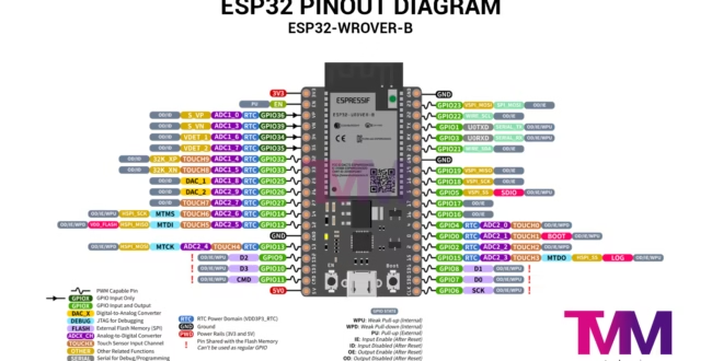
ESP32-WROVER Pinout Description
The ESP32-WROVER has the same pinout as the ESP32-WROOM. The pins are categorized into digital pins, analog pins, and power pins. Refer to the table below for details on pins with secondary functions. Moreover, these secondary pins often serve communication purposes, such as I2C and SPI or as ADC channels.
| Pin Name | Description | Pin Name | Description |
|---|---|---|---|
| 3V3 | 3.3 V power supply | GND | Ground |
| EN | CHIP_PU, Reset | IO23 | GPIO23 |
| VP | GPIO36, ADC1_CH0, S_VP | IO22 | GPIO22 |
| VN | GPIO39, ADC1_CH3, S_VN | TX | GPIO1, U0TXD |
| IO34 | GPIO34, ADC1_CH6, VDET_1 | RX | GPIO3, U0RXD |
| IO35 | GPIO35, ADC1_CH7, VDET_2 | IO21 | GPIO21 |
| IO32 | GPIO32, ADC1_CH4, TOUCH_CH9, XTAL_32K_P | GND | Ground |
| IO33 | GPIO33, ADC1_CH5, TOUCH_CH8, XTAL_32K_N | IO19 | GPIO19 |
| IO25 | GPIO25, ADC1_CH8, DAC_1 | IO18 | GPIO18 |
| IO26 | GPIO26, ADC2_CH9, DAC_2 | IO5 | GPIO5 |
| IO27 | GPIO27, ADC2_CH7, TOUCH_CH7 | IO17 | GPIO17 3 |
| IO14 | GPIO14, ADC2_CH6, TOUCH_CH6, MTMS | IO16 | GPIO16 3 |
| IO12 | GPIO12, ADC2_CH5, TOUCH_CH5, MTDI | IO4 | GPIO4, ADC2_CH0, TOUCH_CH0 |
| GND | Ground | IO0 | GPIO0, ADC2_CH1, TOUCH_CH1, Boot |
| IO13 | GPIO13, ADC2_CH4, TOUCH_CH4, MTCK | IO2 | GPIO2, ADC2_CH2, TOUCH_CH2 |
| D2 | GPIO9, D2 2 | IO15 | GPIO15, ADC2_CH3, TOUCH_CH3, MTDO |
| D3 | GPIO10, D3 2 | D1 | GPIO8, D1 2 |
| CMD | GPIO11, CMD 2 | D0 | GPIO7, D0 2 |
| 5V | 5 V power supply | CLK | GPIO6, CLK 2 |
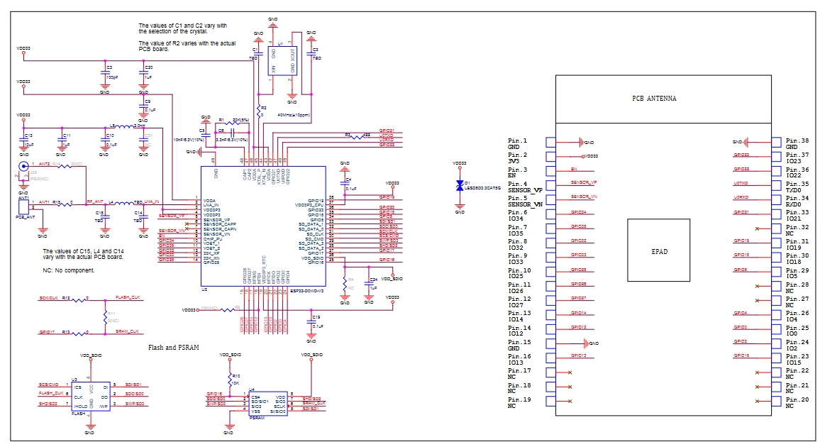
ESP32 WROVER Schematic Diagram
The schematic diagram below is a useful reference, together with the pinout as you make your project.
Do you want some ESP32 project ideas? Check out the following tutorials:
- Sensor Display on ESP32 Web Server
- ESP32 Turbidity Sensor
- ESP32 Magnetometer using HMC5883L
- ESP32 MAX7219 WiFi Message Board
- Using Restful APIs with ESP32
- ESP32 Pressure Sensor
... and many more! See our ESP32 Tutorial archive.


")
