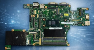
Introduction
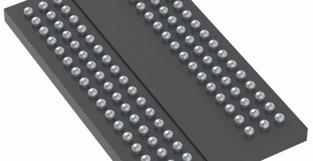
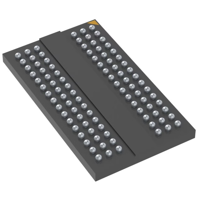
The MT40A512M16LY-075:E is a DDR4 SDRAM with a 96-ball BGA design. This Dynamic Ram module 8n-prefetch architecture to perform operations at high speeds, combined with an interface designed to transfer two data words per clock cycle at the I/O pins.
This configuration of the MT40 SDRAM offers a data transfer rate of up to 2666 MT/s, meaning it can transfer up to 2.666 billion data transfers per second, and since it's a DDR memory, its effective clock frequency is 1333 MHz.
The Core Logic and the I/O Buffer require a stable voltage rating between 1.14 to 1.26 VDC with a tolerance of 60mV. Required for DRAM cell access, the MT40A512M16LY-075:E has a separate high voltage supply with a rating of 2.5 V ± 250 mV needed to drive memory word lines in memory cells.
Design Analysis
● Memory Addressing
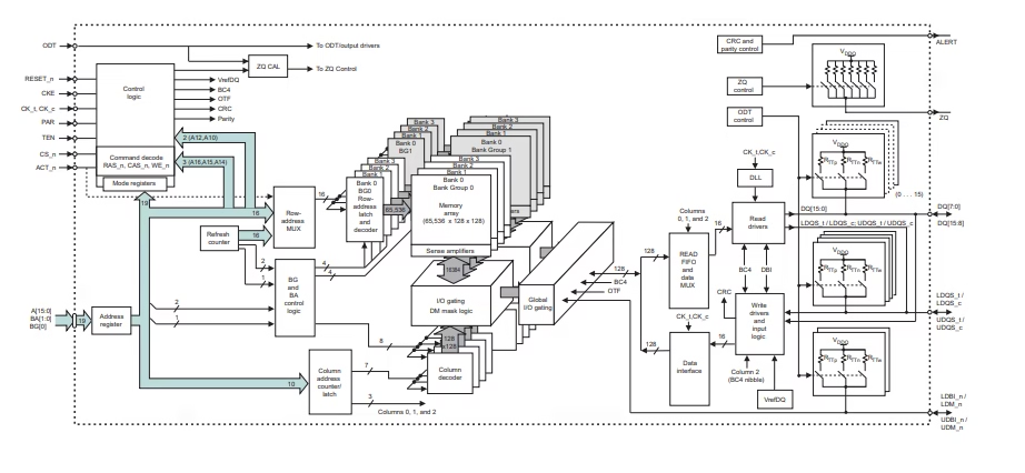
Bank Groups: This DDR4 RAM has 2 Bank groups, where the memory is divided into two arrays, improving data access times and reducing conflicts. To select between the Bank groups, only one 1 address Bit (BG0) is required to make the selection.
Bank Group Addressing: Each Bank group has 4 banks, equalling a total of 8 banks with 2 bits (BA0 or BA1) required to select 4 banks within a group.
Row Addressing: Each bank contains exactly 65,536 rows that can be used to store pages of data with read and write capability. The Row addressing uses 16 bits (A0:A15).
Column Addressing: Similar to Rows storing data for read/write purposes, the Column address has around 1024 columns, with 10-bit addressing (A0:A9).
Page Size: Used for memory management, in MT40A512M16LY-075:E, the page size is:
1024 columns × 16 bits ÷ 8 = 2048 bytes = 2 KB per bank.
● State Diagram
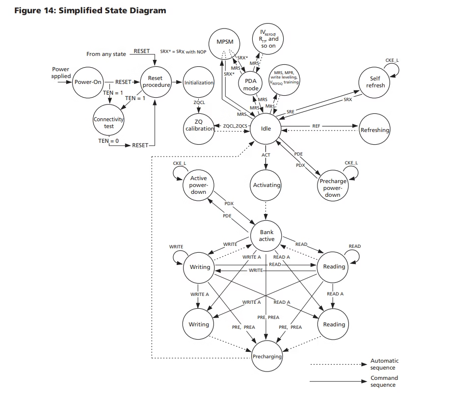
Under Normal Operation mode, this SDRAM module functions in the following sequence:
Power-On → Initialization → Idle → Activate → Read/Write → Precharge → Idle
- Power-On / Reset: Voltage of the device stabilizes, resetting all the logic states of the device.
- Initialization: During the initialization phase, the memory controller programs the Mode registers
- Idle/Standby: The memory banks are all charged and waiting for commands. This is also known as the “Ready State”.
- Activation Phase: In a specific Bank, a Specific Row is used with data being used from it to be loaded into sense amplifiers. This takes place before any reading or writing operation.
- Read/Write: During an active memory transaction, actual data transfer takes place from an active Row.
- Precharge Phase: When waiting for the next set of commands, the memory bank closes its active row. This usually happens between read/write cycles.
- Self-Refresh: When in low power or idle mode, the DRAM will refresh its memory banks internally to ensure smooth future operation.
- Power Down: This is the last phase, when the clock input is disabled and the internal logic is halted, but the data is retained.
Conclusion
The MT40A512M16LY-075:E offers a lot of memory processing power and has tons of other features that add to its intricate design, making it a good choice for various embedded systems designs. If the architecture for MT40A512M16LY-075:E is too complex, check out our article on DDR3 and DDR4 Memory chips to learn more. To source an MT40A512M16LY-075:E DDR4 SDRAM, visit Flywing-tech.com