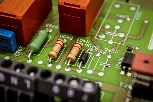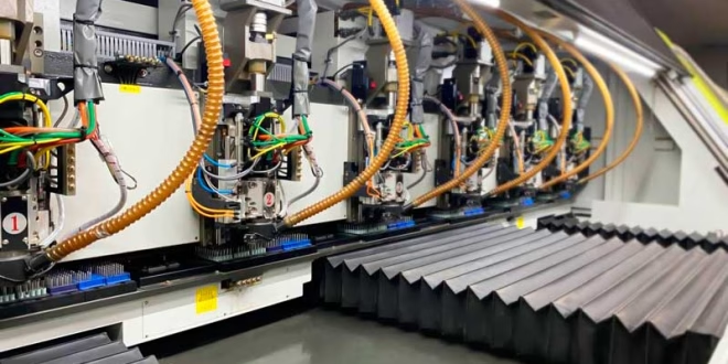
A microcontroller project often begins with a development board, a breadboard, and several jumper wires. Once the circuit and firmware work as expected, the next step is usually a custom printed circuit board that can support repeatable testing, installation, or product development.
Preparing a board for custom PCB Manufacturing requires more than exporting Gerber files from PCB design software. Designers also need to verify the schematic, review component footprints, prepare assembly data, and decide how the finished board will be programmed and tested. A structured microcontroller PCB production checklist can prevent many problems before fabrication begins.
1. Verify the Schematic Before Preparing Production Files
The schematic remains the foundation of the finished board. A circuit that works on a breadboard may still contain assumptions that create problems on a custom PCB.
Start by checking the microcontroller’s supply voltage, current requirements, reset circuit, clock source, and programming interface. Confirm that every power pin has the correct connection and that decoupling capacitors are placed around the device according to the component documentation.
The review should also cover:
- Pull-up and pull-down resistors
- Voltage regulator input and output capacitors
- Logic-level compatibility between connected devices
- Protection components on exposed inputs
- Communication interfaces such as UART, I2C, SPI, CAN, and USB
- Connector pin assignments
- Status LEDs and current-limiting resistors
It helps to label important signals clearly. Consistent net names make it easier to compare the schematic with the PCB layout and later troubleshoot the assembled board.
2. Confirm Every Component Footprint
A correct schematic can still produce an unusable PCB when the physical footprints are wrong. Before releasing the design, compare each footprint with the latest component datasheet.
Check Package Dimensions
Verify pad size, pin pitch, package orientation, and mechanical dimensions. Components with similar names may use different packages, even when their electrical functions are identical.
Pay Attention to Polarity and Pin 1
Diodes, LEDs, electrolytic capacitors, ICs, and connectors require clear orientation markings. The silkscreen should make Pin 1 and polarity easy to identify during assembly and manual inspection.
Review Connectors Mechanically
Connector problems often become visible only after the board arrives. Check whether cables can be inserted without interference from nearby components, mounting hardware, or the enclosure.
3. Run a Final PCB Layout and DFM Check
A design rule check can identify clearance violations, unconnected nets, and layout errors. A manual review is still useful because automated checks cannot understand every mechanical or functional requirement.
Important areas to examine include:
- Minimum trace width and spacing
- Via diameter and drill size
- Copper-to-board-edge clearance
- Solder mask openings
- Annular ring dimensions
- Mounting-hole positions
- Component spacing
- Board outline and cutouts
- Reference designator placement
For microcontroller boards, place decoupling capacitors close to their related power pins. Keep crystal traces short, and follow appropriate routing practices for USB, Ethernet, high-speed memory, or other timing-sensitive signals.
The board should also include accessible test points for important power rails, ground, reset, and communication signals. These points can save significant troubleshooting time after assembly.
4. Prepare and Review the Gerber Package
Gerber files describe the copper, solder mask, silkscreen, and mechanical layers used during fabrication. A typical manufacturing package includes:
- Top and bottom copper layers
- Internal copper layers for multilayer boards
- Top and bottom solder mask
- Top and bottom silkscreen
- Board outline
- Plated and non-plated drill files
- Fabrication notes when required
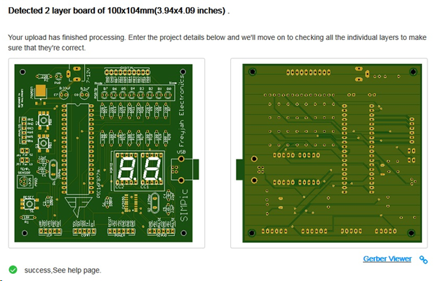
Inspect the Files in a Gerber Viewer
Open the exported package in an independent Gerber viewer. Inspect every layer instead of relying only on the PCB editor.
Check that the board outline is closed, drill locations align with pads, text has the correct orientation, and all required layers are present. Confirm that copper pours were generated correctly and that no design elements extend beyond the intended board boundary.
File names should also be clear enough for the manufacturer to identify each layer without guessing.
5. Build an Assembly-Ready Bill of Materials
The bill of materials, or BOM, tells the assembler which components belong on the board. Each populated component should include enough information to identify and source the correct part.
Useful BOM fields include:
- Reference designator
- Quantity
- Component description
- Manufacturer
- Manufacturer Part Number
- Package or footprint
- Supplier Part Number
- Approved alternative
- Special assembly notes
Avoid descriptions such as “10 kΩ resistor” without specifying package, tolerance, power rating, and other relevant characteristics. Several parts can share the same basic value while having very different physical or electrical specifications.
When the same provider such as WonderfulPCB also handles assembly, supplying a complete BOM and accurate placement data lets fabrication, component sourcing, and assembly run from one release package.
6. Export Accurate Placement Data
Automated assembly equipment uses centroid or pick-and-place files to determine where each component belongs. These files normally include the reference designator, X and Y coordinates, rotation, and board side.
Confirm Rotation Conventions
Rotation values can vary between design tools and assembly systems. Include an assembly drawing that shows the expected orientation of ICs, diodes, LEDs, connectors, and polarized capacitors.
Mark Components That Should Remain Unpopulated
If the PCB contains optional or development-only parts, identify DNP or “do not populate” components clearly in both the BOM and assembly documentation. Conflicting files can cause avoidable production questions or assembly errors.
7. Plan Firmware Programming Before Production
Programming access should be considered during PCB design. Once components are assembled and the board is installed in an enclosure, reaching small programming pads may become difficult.
Depending on the microcontroller, the board may need:
- SWD headers for ARM-based devices
- ICSP connections for PIC microcontrollers
- JTAG access
- UART bootloader pins
- USB programming access
- BOOT and RESET controls
Production quantities may justify dedicated programming pads and a pogo-pin fixture. Smaller prototype batches can use headers or exposed test pads, provided that the connections remain accessible.
The programming plan should identify who loads the firmware, which version should be used, and whether configuration data or device-specific identifiers must also be written.
8. Define an Assembly Testing Procedure
A finished PCBA should go through a controlled power-up and testing process. Applying power immediately without checking the board can turn a minor assembly issue into damaged components.
A basic microcontroller board test sequence may include:
- Visually inspect component placement and solder joints.
- Check resistance between the main power rail and ground.
- Apply power with a current-limited supply.
- Measure each regulated voltage.
- Confirm that the reset and clock circuits operate correctly.
- Connect the programming tool and identify the microcontroller.
- Load test firmware.
- Test GPIO, sensors, communication ports, and other interfaces.
- Record the result and any observed failure.
The exact test procedure should match the board’s intended function. A sensor controller may need calibrated input tests, while a motor-control board may require staged testing before connecting a load.
9. Begin With a Prototype Batch
A prototype batch allows the engineering team to evaluate the physical PCB, assembly quality, firmware behavior, connector access, and enclosure fit before committing to a larger order.
During prototype validation, document every required change. Even minor findings—such as unclear silkscreen labels, inconvenient test points, or connectors placed too close to the board edge—can improve the next revision.
After the prototype passes electrical, functional, and mechanical testing, the files can be released for a larger production run with greater confidence.
Final Microcontroller PCB Production Checklist
Before submitting a microcontroller board for production, confirm that:
- The schematic has been reviewed.
- Power, reset, clock, and programming circuits are correct.
- Every component footprint matches its datasheet.
- PCB design rules and mechanical clearances have been checked.
- Gerber and drill files have been inspected.
- The BOM contains complete part information.
- Pick-and-place data matches the assembly drawing.
- DNP components are clearly identified.
- Programming connections are accessible.
- A board testing procedure has been prepared.
- The first order uses an appropriate prototype quantity.
FAQ
What files are required for microcontroller PCB manufacturing?
Most manufacturers require Gerber files, drill files, and fabrication notes. PCB assembly also requires a BOM, pick-and-place file, and assembly drawing. Complex boards may need additional mechanical or testing documentation.
Does a PCB assembler need the firmware?
Firmware is only required when the assembler is expected to program or functionally test the microcontroller. The programming file, device settings, procedure, and acceptance criteria should be supplied together.
Why is a pick-and-place file important?
A pick-and-place file gives automated assembly equipment the coordinates, rotation, and board side for each component. Incorrect placement data can lead to orientation errors or production delays.
Should a new microcontroller PCB begin with a prototype batch?
Yes. A prototype batch provides an opportunity to verify electrical performance, firmware programming, assembly quality, connector placement, and enclosure fit before scaling production.
Can WonderfulPCB handle both PCB manufacturing and assembly?
WonderfulPCB offers PCB fabrication and assembly as part of its electronic manufacturing services. Combining the two stages can simplify file coordination, component sourcing, and production communication for custom microcontroller boards.