Introduction: The Role of Solder in PCB Assembly
In every pcb assembly process, solder is the invisible champion—creating robust mechanical and electrical connections that bring electronic components and circuits to life. As electronic devices shrink and their functionality grows, the precision of the soldering process becomes more critical than ever. Whether you’re designing high-speed digital boards, power-heavy industrial modules, or medical instruments, mastering pcb assembly and soldering is non-negotiable for performance and reliability.
What is a Printed Circuit Board (PCB)?
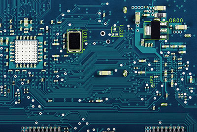
A printed circuit board (PCB) is a layered platform made of a non-conductive substrate (like FR-4) and copper traces, designed to connect, support, and interface with a variety of electronic and semiconductor components. The surface mount or through-hole mounting of components—using solder—is what turns a blank substrate into a functional electronics brain.
PCB Design, Materials, and Fabrication
| PCB Assembly Aspect | Description |
|---|---|
| PCB Design | Involves layout of copper traces, pads, and vias to connect and power electronic circuits |
| Substrate | FR-4, Rogers, aluminum, PTFE, blends—picked for cost, electrical, and thermal properties |
| Copper Cladding | Defines signal, power paths; can be single- up to 32+ layers for high-density electronics |
| Solder Mask | Protects copper during wave and reflow; prevents shorts by guiding solder flow |
| Surface Finishes | ENIG, HASL, OSP, silver—affects solderability, cost, and assembly process |
The pcb manufacturing process includes creating these layers through steps like chemical etching, CNC drilling, laser cutting, and applying solder mask. Assembling and soldering components transforms this “bare” board into a smart system.
PCB Assembly Methods and the PCB Manufacturing Process
Surface Mount Technology (SMT) Assembly
Modern surface mount technology (SMT) dominates high-volume manufacturing for its efficiency, manufacturability, and ability to densely populate both sides of a board with small SMD components. SMT assembly uses automated assembly lines, stencils for precise solder paste application, pick-and-place robots, and controlled reflow ovens.
SMT Assembly Process Steps
| Step | Key Details |
|---|---|
| Stencil Printing | Applies solder paste via laser-cut steel stencils on PCB surface |
| Placement | Automated machines precisely set chips, resistors, capacitors |
| Reflow | Heats assemblies to melting point, forms solder joints |
| AOI Inspection | High-speed cameras detect assembly defects, alignment issues |
PCB design for SMT calls for close attention to pad size, solder mask clearances, and thermal relief networking. This maximizes manufacturability and minimizes process defects like tombstoning or solder bridging.
Through-Hole Technology and Hybrid Assembly
Through-hole technology is favored in applications requiring high current, mechanical durability, or modular upgrades. Here, component leads are inserted into drilled holes and soldered, usually by wave soldering; it still has an important place in mixed-technology assemblies.
Hybrid and Mixed Assembly Approaches
Mixed board assembly uses both surface mount and through-hole components—first populating SMDs, then performing selective soldering or wave soldering for THT parts. This allows for optimal circuit miniaturization and mechanical robustness, especially in power modules and industrial controllers.
Manual, Automated, and Turnkey Assembly Approaches
Manual and Hand Soldering
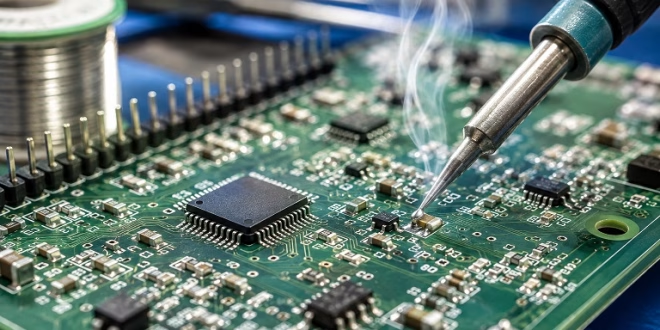
Hand soldering, or manual soldering, is indispensable for prototyping, rework, or specialized repairs where automated process equipment is impractical. In these builds, a skilled technician uses a soldering iron, flux, and keen eyes to ensure quality.
Automated and Turnkey PCB Assembly
Modern assembly lines—including laser soldering and selective soldering with precision nozzles—allow for high throughput, consistency, and process control. Turnkey PCB services source components, fabricate the board, assemble, and test—all under one roof, ensuring streamlined supply chains.
Essential Soldering Tools and Assembly Equipment
Success in pcb assembly relies on both skill and proper tools.
- Soldering Iron or Soldering Station: Delivers the right thermal profile for each soldering process; digital models allow precise temperature control crucial for different alloys.
- Solder Paste and Solder Wire: Available in leaded and lead-free options, with different melting points and flux systems.
- Flux & Soldering Flux: Removes oxides, improves solder flow, and forms reliable solder connections. The right flux for each assembly is vital to prevent flux residue or process contamination.
- Wave Soldering Machine: used in high-volume through-hole assembly lines.
- Automated Pick-and-Place: Optimizes placement speed and accuracy for SMT assembly.
- Stencil Printers: For even, controlled solder paste deposition (important for both reflow and wave/reflow combos).
- Selective Soldering Equipment: CNC-controlled soldering with specialized nozzle for complex hybrid assemblies.
- Hand Tools: Solder sucker, wick, ESD-safe tweezers, magnification system, and a soldering clamp.
Soldering Techniques for Board Assembly
Proper selection and execution of soldering techniques are fundamental to ensuring mechanical and electrical reliability. Let's review and compare the main soldering methods:
Reflow Soldering Process
The reflow soldering process is central to SMT assembly. After solder paste application, electronic components are placed, then the board moves through a reflow oven with controlled thermal zones:
| Reflow Stage | Temp Range | Function | Soldering Tip |
|---|---|---|---|
| Preheat | 120–150°C | Gradual heating, activates flux | Ramp slowly |
| Soak | 150–180°C | Outgasses volatiles, evens temp | Avoid spatter |
| Reflow Peak | 230–250°C | Solder melts, alloy bonds form | Don’t overheat |
| Cooling | Controlled | Solidifies robust solder joints | Steady, slow |
Best practices for reflow include optimizing PCB design for thermal balance, choosing the correct solder paste alloy for your components, and careful process control.
Wave Soldering
Wave soldering is a staple of high-throughput assembly lines and is essential for robust through-hole technology and certain mixed SMT assemblies. During the wave soldering process, assembled boards are preheated, have flux applied, and are then passed over a carefully defined wave of molten solder. This ensures that every joint is wetted uniformly, producing consistent solder joints and electrical connections for all inserted leads in one swift automated process.
Key Attributes of Wave Soldering:
- Ideal for large-scale pcb assembly or fabrication and assembly where high reliability is critical.
- Suitable for power modules, connectors, and industrial circuits exposed to repeated mechanical and thermal stress.
- Further process control can be achieved using nitrogen blanketing over the solder bath to minimize oxidation.
Wave Soldering Best Practices:
- Adjust conveyor speed and wave height for optimal solder penetration.
- Regularly monitor melting point and actual alloy composition in the solder pot.
- Clean flux residue from the board surface promptly to prevent corrosion.
- Use automated inspection to catch assembly defects such as bridging, icicle formation, or poor solder flow.
Selective Soldering
Selective soldering is an advanced solution for modern demanding pcb assembly methods, particularly for mixed-technology board assembly. When only specific through-hole components need to be soldered after an SMT reflow, selective soldering is used. A localized nozzle delivers a precisely controlled stream of molten solder directly to the pad and lead interface.
Benefits of Selective Soldering:
- Reduces risk of thermal stress and reflow damage to already-soldered SMT parts.
- Allows for compact, high-component-density circuits that combine the best of both SMT and through-hole parts.
- Advanced flux application and programmable preheating profiles boost overall assembly quality and joint formation.
Hand, Laser, and Manual Soldering
Hand soldering and manual soldering remain essential in several manufacturing solutions:
- Prototypes and low-volume production where setup of automated assembly processes is not viable.
- PCB repair or rework situations, such as after in-circuit testing or repairs of field failures.
- For very specialized or sensitive electronic circuits, such as those found in aerospace or R&D settings.
Hand Soldering Tips:
- Use an ESD-safe, temperature-controlled soldering iron tailored to your solder alloy’s melting point.
- Pick the right tip for the job: fine for SMT, chisel for THT.
- Always use compatible, high-quality flux to ensure good solder flow.
- Avoid prolonged heat exposure to prevent lifted pads or board warpage.
Laser soldering is an emerging precision technique for microelectronic assembly and advanced PCB manufacturing solutions, especially for small-format PCBs and devices where mechanical or thermal shock from other methods could damage sensitive semiconductors or substrates.
Quality Control, Defects, and How to Troubleshoot
Ensuring perfect solder joints and eliminating assembly defects is at the core of professional PCB assembly and soldering.
Common Defect Types in Soldering Process:
| Defect Type | Cause | Detection & Solution |
|---|---|---|
| Cold Joint | Low heat, insufficient flux/solder | Rework with more solder and heat |
| Solder Bridge | Excess solder or poor stencil design | Remove with solder wick/sucker |
| Tombstoning | Uneven heating for small SMD parts | Adjust reflow profile |
| Voids | Outgassing from dirty boards or paste | Bake PCB prior to assembly, X-ray |
| Incomplete Wetting | Oxidation, poor flux action | Use fresh, suitable flux |
| Cracking | Excessive thermal stress | Gradual cooling, tweak oven settings |
Inspection methods—such as Automated Optical Inspection (AOI), X-ray inspection, and electrical testing—are mandatory to verify soldering quality, catch hidden faults, and guarantee long-term circuit reliability.
Repair and Troubleshooting
If a defect is found:
- Identify affected joints visually and with electrical probing.
- Desolder with a soldering iron and remove old solder using a solder sucker or wick.
- Apply new flux and resolder, ensuring good solder flow and correct alloy selection.
- Clean flux residue thoroughly to prevent ionic contamination.
- Document the defect and corrective action taken for ongoing process improvement.
The Role of Nitrogen, Flux, and Solder Alloys
Nitrogen’s inert properties, when introduced into the soldering process (wave, reflow, or selective methods), allow for:
- More consistent wetting and shinier, stronger solder joints
- Less dross and reduced oxidation—essential for assembly in aerospace and demanding commercial applications.
Flux comes in multiple forms—rosin, no-clean, water-soluble—and is matched to the specific alloy, assembly process, and cleaning requirement. Always choose flux that fits your production environment and application (e.g., no-clean for consumer, water-soluble for high-reliability).
Properties and Types of Solder/Alloy
- Lead-free solder (typically SAC305) dominates in modern electronics for health, safety, and environmental reasons.
- Tin-lead alloys are still used for legacy and some specialized applications, known for their low melting point and forgiving soldering characteristics.
- Silver/copper-containing alloys are leveraged when mechanical and electrical reliability must be maximized.
Always check thermal properties, melting point, and compatibility with your circuit and assembly lines.
Advanced Trends & Manufacturing Solutions
The drive for miniaturization, performance, and environmental responsibility has inspired new pcb manufacturing and soldering techniques:
- 3D AOI/AI-based Inspection: Detects fine-pitch or internal defects that traditional methods might miss.
- Environmentally-friendly soldering: Focus on reducing waste, using recyclable materials, and integrating lead-free alloys.
- Digital process control: Real-time logging of soldering profiles, oven temperatures, and nitrogen purity improves future board assembly yield and reliability.
- Laser cutting and laser soldering: Support for micro-sized components and precise rapid prototyping in advanced facilities.
Top Tips for PCB Assembly Soldering Success
- Maintain Cleanliness: Clean PCBs and fresh flux ensure proper solder flow and robust electrical connections.
- Temperature Control: Always match soldering iron or oven profiles to alloy specifications and board stack-up.
- Select the Right Solder Paste/Alloy: Modern, high-performance circuits demand lead-free, reliable solder pastes.
- Optimize PCB Design: Good pad design, thermal relief, and trace layout boost manufacturability and minimize defects.
- Protect Sensitive Assemblies: Use ESD protection, careful handling, and nitrogen for the cleanest, strongest results.
- Log Every Defect: Build a process control data logbooks—feedback is the fastest route to high assembly quality.
- Invest in Automated Inspection for all high-value boards—an extra minute on AOI or X-ray pays for itself many times over in field reliability.
Conclusion & Next Steps
Solder is the silent hero that enables every leap in electronic design and manufacturing. By understanding the range of soldering methods, the science behind alloys and flux types, and the nuances of reflow, wave soldering, selective soldering, and manual soldering, designers and assembly experts lay the foundation for world-class product reliability.
Modern pcb assembly integrates sophisticated inspection, process control, and environmentally responsible materials—led by soldering experts who combine technology with the art of perfecting robust electrical connections.
If you're ready to guarantee the performance, reliability, and manufacturability of your next product—embrace continuous improvement in your soldering process, leverage the latest technology, and consult qualified partners for turnkey PCB and advanced electronic manufacturing solutions.
Ready to build the future, one reliable solder joint at a time? Contact us for a custom quote, expert technical review of your PCB design and manufacturing plan If you want guidance on complex assembly approaches or access to cutting-edge manufacturing solutions—including turnkey PCB, micro-assembly for IoT, or advanced wave and reflow combinations—partner with a proven pcb assembly and soldering expert. Today’s best providers leverage every aspect of the soldering process, from automated lines for high-volume to precision hand soldering for critical repairs and manual soldering on prototypes or complex hybrid board assembly.
Why Trust Professionals for PCB Fabrication and Assembly?
- Access to cleanrooms and calibrated equipment for consistent assembly quality
- Proven history with high-end markets: medical, aerospace, energy
- Advanced tools for nitrogen-controlled wave soldering, precision reflow, and selective soldering with computer-controlled nozzles
- Comprehensive post-assembly inspection with AOI and X-ray to ensure zero-defect shipments
- Support at all phases of design and manufacturing, from PCB design DFM review to end-of-line test and traceability
Case in Point: A European electric vehicle startup reduced warranty claims by 70% after switching to an assembly partner specializing in nitrogen-assisted wave soldering and advanced flux chemistry—solving chronic corrosion and thermal stress issues on mixed-technology PCBs.
Frequently Asked Questions About PCB Assembly Soldering
1. How are PCBs soldered?
PCBs are typically soldered using reflow soldering, wave soldering, selective soldering, or manual soldering. The appropriate method depends on the component type, PCB design, production volume, and assembly requirements.
2. What are the main soldering techniques used in PCB assembly?
Common PCB soldering techniques include reflow soldering for SMT components, wave soldering for through-hole components, selective soldering for targeted areas, and hand soldering for prototypes, repairs, or low-volume assembly.
3. What kind of solder is used for PCB assembly?
PCB assembly commonly uses lead-free solder alloys such as SAC305 or traditional tin-lead alloys such as Sn63/Pb37 where permitted. The choice depends on regulatory requirements, operating conditions, and manufacturing processes.
4. What is the ideal temperature for soldering PCBs?
For hand soldering, tip temperatures are commonly around 315–350°C for leaded solder and 330–370°C for lead-free solder. The exact temperature should be adjusted according to the solder alloy, component size, and PCB thermal mass.
5. What is wetting in PCB soldering?
Wetting occurs when molten solder properly spreads across and bonds to the component lead and PCB pad. Good wetting produces a reliable electrical and mechanical solder joint.
6. Why won’t solder stick to a PCB?
Poor solder adhesion can result from oxidation, contamination, insufficient flux, inadequate heating, or damaged surface finishes. Proper cleaning, flux application, and temperature control usually improve solder wetting.
7. What are the most common PCB soldering defects?
Common defects include solder bridges, cold joints, insufficient solder, solder balls, voids, non-wetting, tombstoning, and lifted pads. Proper process control and inspection help prevent these issues.
8. Can soldering damage a PCB?
Yes. Excessive temperature or prolonged heating can lift pads, damage components, degrade laminate materials, or cause PCB delamination. Controlled temperature and heating time are essential during soldering and rework.
9. Can too much flux cause PCB soldering problems?
Yes. Excessive flux can leave residues, contaminate the PCB, interfere with inspection, and in some cases affect long-term reliability. The correct flux type and controlled application should be used for the soldering process.
10. What is Class 3 soldering in PCB assembly?
Class 3 refers to the highest performance category defined by IPC standards for electronic assemblies where continued operation and reliability are critical. It requires stricter workmanship and solder-joint acceptance criteria than Class 1 or Class 2 products.