The ESP32-S3 analog-to-digital converter works well with low-impedance voltage sources. However, problems can appear when the analog signal comes from a high-value resistor divider, a resistive sensor, or another circuit that cannot supply much current.
You may notice that the measured voltage is lower than expected, the first reading is different from the following readings, or one ADC channel appears to affect another. These symptoms are often blamed on analog input leakage current. Leakage is part of the problem, but the ESP32-S3's switched-capacitor ADC input also creates a temporary load whenever a conversion starts.
In this article, we will examine how ESP32-S3 analog input leakage affects high-impedance circuits and how to design an ADC input that produces stable and repeatable readings.
How the ESP32-S3 ADC Input Works
The ESP32-S3 contains two 12-bit successive-approximation ADC units. Together, they provide 20 analog input channels:
| ADC Unit | Channels | GPIO Pins |
|---|---|---|
| ADC1 | ADC1_CH0 to ADC1_CH9 | GPIO1 to GPIO10 |
| ADC2 | ADC2_CH0 to ADC2_CH9 | GPIO11 to GPIO20 |
For most projects, ADC1 is the better choice. Espressif recommends ADC1, and ADC2 analog functions cannot be used normally while Wi-Fi is using the ADC2 peripheral.
A 12-bit conversion produces values from 0 to 4095. However, the raw result is not automatically equal to an exact voltage because the internal reference voltage varies from one chip to another. The ESP32-S3 reference is designed around 1.1 V, but its actual value can vary approximately from 1.0 V to 1.2 V. For this reason, calibrated voltage functions should be used whenever possible.
What Is Analog Input Leakage Current?
An ideal ADC input would have infinite resistance and draw no current from the measured circuit. A real microcontroller pin contains protection structures, switches, multiplexers, transistors, parasitic capacitance, and internal analog circuitry. Small currents can therefore flow into or out of the pin.
When the source resistance is low, this current produces almost no visible error. When the source resistance is hundreds of kilohms or several megohms, even a tiny current can create a measurable voltage drop.
The approximate DC error caused by leakage is:

For example, suppose an analog source has an equivalent resistance of 200 kΩ. The resulting errors would be:
| Assumed Leakage Current | Voltage Error with 200 kΩ Source |
|---|---|
| 10 nA | 2 mV |
| 50 nA | 10 mV |
| 100 nA | 20 mV |
| 1 µA | 200 mV |
The ESP32-S3 datasheet specifies a maximum high-level and low-level digital GPIO input current of 50 nA under its stated DC test conditions. However, this value should not be treated as a guaranteed ADC input leakage specification. The datasheet does not provide a separate worst-case analog leakage value covering ADC conversions, attenuation settings, temperature, board contamination, and all operating modes.
For a high-impedance design, it is safer to consider the 50 nA figure only as a pin-level reference. The complete ADC circuit should be tested across temperature and operating conditions, or isolated from the signal source using an analog buffer.
The ADC Is a Dynamic Load
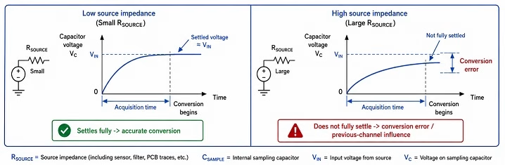
Leakage current explains steady DC error, but it does not explain every problem seen with high-impedance inputs. The ESP32-S3 uses a successive-approximation ADC, which includes an internal sampling network.
At the beginning of a conversion, an internal switch briefly connects the selected GPIO to a sampling capacitor. The input source must provide enough charge for this capacitor to approach the input voltage during the available acquisition period.
A simplified settling relationship is:

Here, Rsource is the source resistance, Csample is the effective internal sampling capacitance, and tacq is the acquisition time.
As the source resistance increases, the capacitor takes longer to charge. If the ADC starts its conversion before the voltage settles, the result can be lower or higher than the actual signal. This effect may appear even when the static leakage current is extremely small.
The internal attenuation network also changes the signal path. Consequently, source loading and conversion error may vary with the selected attenuation setting.
Why the First ADC Reading Can Be Wrong
The ADC input multiplexer connects several analog channels to the same converter. When software changes from one channel to another, the sampling network can retain a small amount of charge from the previous channel.
A low-impedance source quickly replaces this charge. A high-impedance source may require more time. The first reading can therefore be influenced by:
- The voltage previously measured on another ADC channel
- Residual charge in the sampling network
- The selected attenuation setting
- The external filter capacitor
- The time between channel selection and conversion
A common software solution is to perform one dummy conversion after changing channels and discard its result. This helps, but it does not replace proper analog input design.
High-Value Resistor Divider Example
Consider a circuit that measures a supply voltage of up to 15 V. To minimize battery drain, we use a 1 MΩ upper resistor and a 220 kΩ lower resistor.
The voltage presented to the ESP32-S3 is:

At 15 V:

This keeps the input below the ESP32-S3 datasheet's 2.9 V effective calibrated range for the highest attenuation setting.
The divider current at 15 V is:

The ADC does not see 1.22 MΩ as its source resistance. The Thevenin resistance at the divider output is:


This is still a relatively high source impedance. An assumed leakage current of 100 nA would produce approximately:

At the original 15 V input, the equivalent error is multiplied by the divider ratio:

This calculation only estimates static leakage error. Sampling transients, resistor tolerance, ADC error, noise, temperature, and PCB leakage can add further error.
Adding a Capacitor to the ADC Input
Espressif recommends placing a 0.1 µF capacitor between the ADC pin and ground. The capacitor performs two useful functions:
- It filters high-frequency noise before it reaches the ADC.
- It acts as a local charge reservoir for the ADC sampling capacitor.
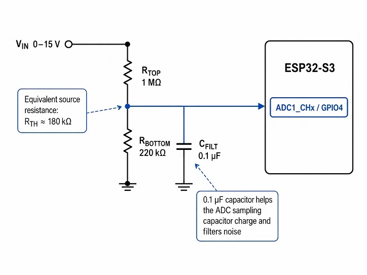
For the 1 MΩ and 220 kΩ divider, the approximate time constant with a 0.1 µF capacitor is:


A capacitor is normally considered nearly settled after about five time constants:

If the divider is permanently connected, the capacitor remains charged and this delay is not usually needed before every measurement. If the divider is switched on only when a reading is required, the firmware should wait approximately 90 to 100 ms before sampling.
The capacitor and divider also create a low-pass filter. Its approximate cutoff frequency is:


This is suitable for battery voltage, temperature, and other slowly changing signals. It may be too slow for audio, vibration, or fast control signals.
Method 1: Reduce the Divider Resistance
The simplest way to reduce loading error is to use lower resistor values. A 100 kΩ and 22 kΩ divider has the same ratio as the 1 MΩ and 220 kΩ divider, but its Thevenin resistance is only about 18 kΩ.
| Divider | Current at 15 V | Thevenin Resistance |
|---|---|---|
| 1 MΩ and 220 kΩ | 12.3 µA | 180.3 kΩ |
| 100 kΩ and 22 kΩ | 123 µA | 18.0 kΩ |
| 47 kΩ and 10 kΩ | 263 µA | 8.25 kΩ |
The lower-value divider consumes more current, but it is less affected by leakage, PCB contamination, and ADC sampling transients.
For mains-powered equipment, the additional current may not matter. For a battery-powered sensor that sleeps most of the time, a switched divider may provide a better compromise.
Method 2: Use a Switched Voltage Divider
A switched divider keeps the resistors disconnected while the ESP32-S3 is sleeping. The firmware enables the divider shortly before taking a measurement and disables it afterward.
A high-side P-channel MOSFET or a low-leakage analog load switch can be used to connect the upper resistor to the measured supply. After enabling the circuit, wait for the divider and filter capacitor to settle.
The switch itself must also be selected carefully. MOSFET off-state leakage, gate leakage, and contamination around the ADC node may become significant when using megohm resistors.
A low-side switch should generally be avoided for this application because it can leave the ADC pin connected to the measured voltage through the upper resistor while the lower resistor is disconnected. This can make the pin float, forward-bias protection structures, or create an unexpected current path.
Method 3: Buffer the Signal with an Op-Amp
For very high-impedance sensors, the best solution is usually a voltage follower.
The sensor or resistor network connects to the op-amp input, while the op-amp output drives the ESP32-S3 ADC. The op-amp presents a very high input resistance to the sensor and a low output resistance to the ADC.
Look for the following characteristics:
- Very low input bias current
- Operation from a 3.3 V supply
- Rail-to-rail input and output
- Input common-mode range that includes the measured signal
- Output swing that covers the required ADC voltage range
- Low offset voltage and low drift
- Stability when driving a capacitive load
A small resistor, typically between 100 Ω and 1 kΩ, can be placed between the op-amp output and the ADC capacitor. This resistor isolates the amplifier from the capacitor and can improve stability.
Some sensor types have an impedance so high that they should never be connected directly to a microcontroller ADC. In such cases, an amplifier designed for extremely low input bias current is required.
Method 4: Improve PCB Layout and Cleanliness
At megohm impedance levels, the PCB becomes part of the analog circuit. Flux residue, dust, moisture, solder mask contamination, and fingerprints can create leakage paths comparable to the signal current.
Use these layout practices:
- Keep the high-impedance trace short.
- Place the filter capacitor close to the ESP32-S3 pin.
- Keep the trace away from switching regulators, clocks, USB, and antenna circuitry.
- Avoid routing digital signals parallel to the ADC trace.
- Clean flux residue from the board.
- Use a ground plane around ordinary low-level analog traces.
- For extremely high impedance, consider a driven guard around the sensitive node.
Also make sure that internal pull-up and pull-down resistors are disabled on the ADC pin. These resistors are approximately tens of kilohms and will completely disturb a high-value divider.
Choosing the ADC Attenuation
The ESP32-S3 ADC supports several attenuation settings. Higher attenuation permits a larger voltage at the pin but usually produces more conversion error near the upper end of the range.
| Arduino Setting | Approximate ESP32-S3 Range | Datasheet Effective Calibrated Range |
|---|---|---|
| ADC_ATTEN_DB_0 | Up to approximately 0.95 V | 0 to 0.85 V |
| ADC_ATTEN_DB_2_5 | Up to approximately 1.25 V | 0 to 1.10 V |
| ADC_ATTEN_DB_6 | Up to approximately 1.75 V | 0 to 1.60 V |
| ADC_ATTEN_DB_11 | Up to approximately 3.10 V | 0 to 2.90 V |
The Arduino API continues to use the name ADC_ATTEN_DB_11, while newer ESP-IDF documentation may describe the highest attenuation as 12 dB.
For best accuracy, do not design the divider so that the maximum expected voltage is exactly at the upper ADC limit. Leave margin for supply variation, resistor tolerance, transients, and calibration error.
Arduino ESP32-S3 ADC Example
The following sketch reads a high-value 1 MΩ and 220 kΩ divider connected to GPIO4. GPIO4 is an ADC1 pin on the ESP32-S3.
The circuit should include a 0.1 µF ceramic capacitor from GPIO4 to ground.
#include <Arduino.h>

const uint8_t ADC_PIN = 4;

const float R_TOP = 1000000.0f;
const float R_BOTTOM = 220000.0f;

const uint8_t SAMPLE_COUNT = 32;

uint32_t readAdcMillivolts()
{
    uint64_t total = 0;

    // Dummy conversion to help the ADC input settle.
    (void)analogRead(ADC_PIN);
    delayMicroseconds(500);

    for (uint8_t i = 0; i < SAMPLE_COUNT; i++)
    {
        total += analogReadMilliVolts(ADC_PIN);
        delayMicroseconds(500);
    }

    return (uint32_t)(total / SAMPLE_COUNT);
}

float readInputVoltage()
{
    const uint32_t adcMillivolts = readAdcMillivolts();
    const float adcVoltage = adcMillivolts / 1000.0f;

    return adcVoltage * (R_TOP + R_BOTTOM) / R_BOTTOM;
}

void setup()
{
    Serial.begin(115200);

    analogReadResolution(12);
    analogSetPinAttenuation(ADC_PIN, ADC_ATTEN_DB_11);

    delay(100);
}

void loop()
{
    const uint32_t adcMillivolts = readAdcMillivolts();
    const float inputVoltage =
        (adcMillivolts / 1000.0f) *
        (R_TOP + R_BOTTOM) / R_BOTTOM;

    Serial.printf(
        "ADC: %lu mV, Input: %.3f V\n",
        (unsigned long)adcMillivolts,
        inputVoltage
    );

    delay(1000);
}
The analogReadMilliVolts() function returns a calibrated voltage rather than an uncorrected raw ADC count. Averaging reduces random noise, while the dummy conversion helps after the input multiplexer or attenuation circuitry has changed state.
The code does not compensate for resistor tolerance, leakage, PCB contamination, or gain and offset error in the complete circuit. Final calibration should be performed using a trusted multimeter or voltage reference.
Two-Point Calibration
For better accuracy, apply two known input voltages and record the corresponding ESP32-S3 readings. The corrected voltage can then be represented as:

The gain is:

The offset is:

Store the resulting gain and offset in flash or non-volatile storage. This calibration corrects consistent gain and offset errors, but it cannot fully correct unstable leakage, insufficient settling time, or temperature-dependent errors.
Sampling High-Impedance ADC Channels
Use the following sampling sequence when reading a high-impedance source:
- Enable the divider or sensor power, when applicable.
- Wait for the external RC network to settle.
- Select the ADC channel and attenuation.
- Perform one dummy conversion.
- Take multiple calibrated readings.
- Average or median-filter the samples.
- Disable the measurement circuit when finished.
Do not sample faster than the source and filter network can settle. Increasing the sample rate does not improve a circuit whose source cannot recharge the ADC input between conversions.
If several ADC channels have very different voltages, consider reading each channel twice and discarding the first conversion. A buffer amplifier for each high-impedance channel provides a more reliable solution.
Wi-Fi and ADC Noise
ADC1 can be used while Wi-Fi is active, but wireless transmission causes rapidly changing current consumption. These current pulses can introduce noise into the power and ground networks.
For precision measurements:
- Use ADC1 instead of ADC2.
- Add proper supply decoupling near the ESP32-S3.
- Place the ADC capacitor close to the pin.
- Avoid taking critical readings during Wi-Fi transmission.
- Average several readings.
- Consider temporarily stopping wireless activity during calibration or precision sampling.
The ESP32-S3 datasheet's ADC characterization was performed with a 100 nF capacitor, a DC input signal, an ambient temperature of 25 °C, and Wi-Fi disabled. A real application may therefore show more noise than the published test results.
Common ESP32-S3 High-Impedance ADC Problems
| Symptom | Likely Cause | Recommended Fix |
|---|---|---|
| Reading is consistently low | Leakage or insufficient acquisition settling | Lower source resistance, add a capacitor, or use a buffer |
| First reading is different | Residual charge from another channel | Discard the first conversion |
| Reading changes when touched | Input is floating or extremely high impedance | Add a defined bias path and buffer the signal |
| Channels affect each other | Multiplexer charge and insufficient settling | Slow the sampling sequence or buffer each channel |
| Voltage changes in humid conditions | PCB surface leakage | Clean the board and improve guarding |
| Large spikes during wireless activity | Supply or ground noise | Improve decoupling, layout, and sampling timing |
| Upper voltage range is inaccurate | Operating near the attenuation limit | Change the divider ratio and add voltage margin |
ESP32-S3 High-Impedance ADC Design Checklist
- Prefer GPIO1 to GPIO10 on ADC1.
- Keep the maximum ADC voltage below the calibrated effective range.
- Add approximately 0.1 µF between the ADC pin and ground.
- Calculate the divider's Thevenin resistance.
- Estimate leakage error using the required voltage accuracy.
- Allow at least five external RC time constants after switching the circuit on.
- Discard the first reading after changing channels.
- Average multiple calibrated readings.
- Disable internal pull-up and pull-down resistors.
- Keep the ADC trace short and away from noisy signals.
- Clean the PCB when using megohm impedances.
- Use an op-amp buffer when the sensor impedance is very high.
- Calibrate the complete circuit, not only the ADC.
Conclusion
The ESP32-S3 ADC input should not be treated as an ideal infinite-resistance voltmeter. Static leakage current can create voltage error when the source impedance is high, while the ADC's internal sampling network can temporarily load the signal during each conversion.
A 0.1 µF capacitor at the ADC pin is an important starting point and is recommended by Espressif. However, the capacitor must be combined with adequate settling time, suitable divider values, ADC1 channel selection, averaging, careful PCB layout, and calibration.
For battery monitoring and other slowly changing signals, a high-value divider with a local capacitor may provide acceptable performance. For extremely high-impedance sensors or precision measurements, a low-bias-current op-amp buffer is the more reliable solution.