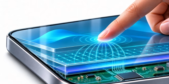
Touchscreens sit on phones, factory HMIs, medical monitors and car dashboards, and most of them sense a finger through capacitance. Tap a screen and a touch controller works out where your fingertip landed from tiny changes in capacitance, scan after scan.
That sensing depends on a layer the user never sees. Between the cover glass and the display sits a patterned film of electrodes that has to carry electrical signals and let light through at the same time. Most conductors are opaque, and most transparent materials are insulators, so a material that does both is unusual.
Indium tin oxide (ITO) has filled that role for decades. Its cost, its brittleness and its sensitivity to process temperature now push engineers to look at other materials, especially for large, flexible and curved displays. This article explains how capacitive sensing works, why the electrode material matters to both the optics and the electronics, and how ITO compares with its alternatives.
How a Capacitive Touchscreen Senses a Finger
Most touchscreens on embedded devices use projected capacitive (PCAP) sensing. A PCAP panel places a grid of transparent row and column electrodes under the cover glass, on a sensor layer that sits between the glass and the display. A touch controller IC drives those electrodes with small excitation signals and measures the capacitance at each electrode or at each crossing.
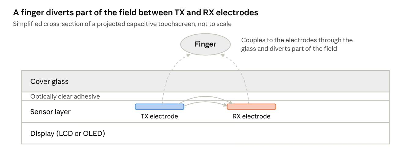
The finger never touches an electrode. The cover glass insulates the sensor from the user, so the finger couples capacitively to the electrodes through the glass. Because human tissue conducts and couples to its surroundings, a nearby fingertip changes the electric field around the electrodes, and the controller reads that change as a change in capacitance.
Field lines between the TX and RX electrodes that reach up through the cover glass are the ones a finger can divert. The controller reads that loss as a drop in mutual capacitance at the crossing.
Controllers measure that change in two ways. Self-capacitance sensing measures each electrode against ground. A finger adds capacitance, so the electrode under it reads higher. The method is simple and sensitive, but in a row-column matrix it only reports which rows and which columns are active. Two fingers light up two rows and two columns, which gives four candidate crossings, and the controller cannot tell the two real touches from the two "ghost" points.
Mutual-capacitance sensing avoids that ambiguity. The controller drives one transmit (TX) electrode at a time and reads the charge that couples into each receive (RX) electrode. A finger near a crossing diverts part of that field, so the coupling at that node drops. Because the controller measures every crossing separately, it can resolve several touches at once, which is what makes true multi-touch possible. Some controllers run both scans, using self-capacitance for sensitivity and mutual capacitance to locate each touch.
Each of those measurements charges an electrode through its own resistance and waits for it to settle before sampling. That step brings the electrode material into the picture.
Transparent Electrodes: What the Material Must Do
The electrode layer has two jobs that pull against each other. It must carry the controller's drive and sense signals with little loss, and it must stay nearly invisible over the display. Engineers rate the first job by sheet resistance, in ohms per square (Ω/sq), and the second by visible transmittance and haze.
Every bit of light the electrode film absorbs is light the display underneath had to produce. In many LED-backlit displays, red light comes from phosphors activated with europium, a rare earth that phosphor makers commonly work with as europium oxide. Researchers have also studied bismuth as a co-dopant in europium-doped yttrium oxide red phosphors for white LEDs.
Sheet resistance ties a film's bulk resistivity to its thickness:

Here Rs is the sheet resistance, ρ is the material's resistivity and t is the film thickness. A film with a resistivity of 2 × 10⁻⁴ Ω·cm and a thickness of 100 nm (1 × 10⁻⁵ cm), for example, has a sheet resistance of 20 Ω/sq. Doubling the thickness halves the sheet resistance, but the thicker film also absorbs and reflects more light. Every sensor design picks a point on that trade-off, and a material with lower resistivity gives the designer a better point to pick.
Resistance matters to the electronics as much as the optics. Each electrode line behaves as a distributed RC network, with the film's resistance along the line and the line's capacitance to neighboring electrodes and the display. The controller has to let each line settle before it samples, so a larger RC product slows the scan or cuts the time left for averaging out noise. Controller design and parasitic capacitance also limit scan speed, but electrode resistance is the part the material choice controls. Larger screens have longer electrode runs, so they need lower sheet resistance to hold the same scan rate and signal-to-noise ratio.
Manufacturers then etch the film into a pattern the controller can address. A common layout uses interlocking diamonds roughly 4 to 8 mm across. One set of diamonds links into rows, the other into columns, and small bridges carry one set over the other at each crossing. Pitch, shape and bridging vary from design to design. Where the film has been etched away, light reflects differently, so the stack has to keep that pattern from showing through the display.
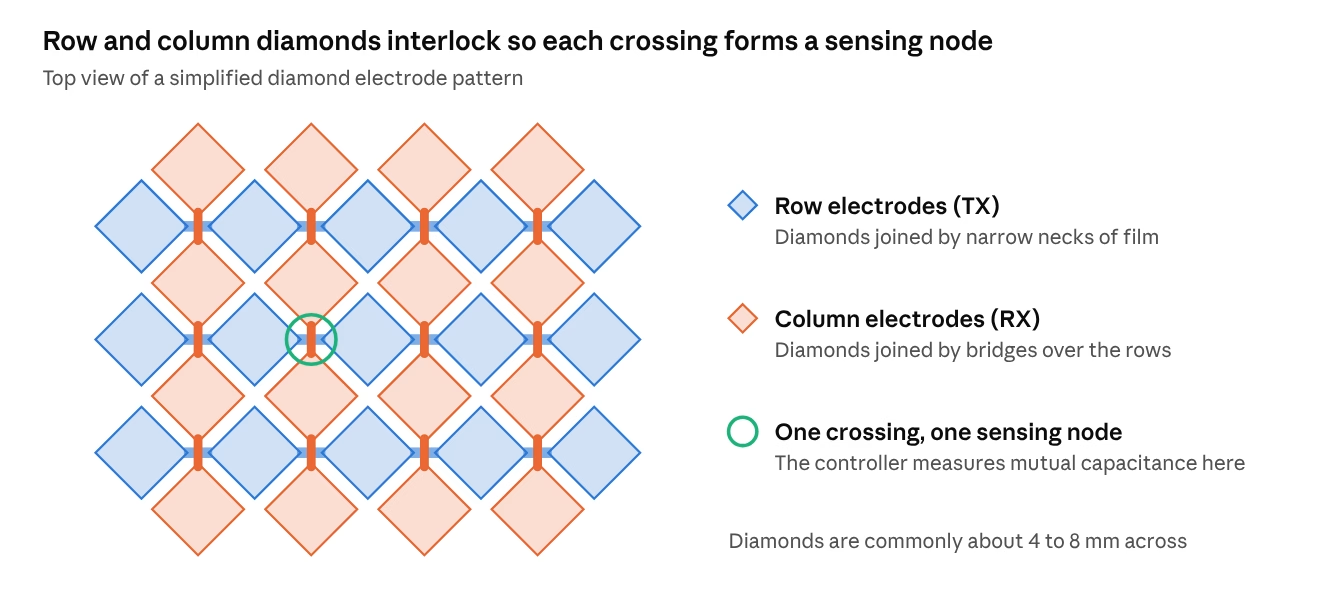
Because the row and column diamonds sit side by side rather than stacked, both sets lie close to the touch surface, and every crossing becomes a node the controller can measure on its own.
For most of the touchscreen era, one material has met these demands best.
Indium Tin Oxide: The Industry Standard
Indium tin oxide is indium oxide (In₂O₃) doped with tin oxide (SnO₂), typically in a ratio of about 90 to 10 by weight. Pure indium oxide is transparent but a poor conductor, and the tin changes that. Each tin ion that takes the place of an indium ion in the crystal lattice donates a free electron, and oxygen vacancies in the film can add more carriers. The result is a degenerate n-type semiconductor with carrier concentrations in the range of 10²⁰ to 10²¹ per cubic centimeter, which behaves electrically almost like a metal.
Optimized ITO films reach a resistivity near 10⁻⁴ Ω·cm. At the same time, ITO's bandgap of roughly 3.5 to 4.3 eV sits above the photon energies of visible light, so visible light passes through with little absorption. Good films commonly transmit more than 85 percent of visible light. That combination, backed by decades of process experience, made ITO the default electrode material.
Panel makers deposit ITO by magnetron sputtering. Argon ions, with a controlled amount of oxygen, strike a dense ceramic ITO target, and the material they knock loose condenses on glass or film. Photolithography and etching then turn the coating into the electrode pattern.
Target quality carries straight into the film. A target with low density or poor homogeneity tends to grow nodules, small dark deposits on its surface, as sputtering goes on. Nodules trigger arcing, and arcs throw particles onto the substrate that become defects in the finished sensor. Target makers work to raise density and control composition for that reason.
ITO also has three well-known limits:
- Supply. Indium comes mainly from zinc ores. China produced about 760 of the world's roughly 1,100 metric tons of refined indium in 2025, close to 70 percent of the total.
- Mechanics. ITO is a ceramic, so it cracks under small tensile strains. Repeated bending grows those cracks until the electrode's resistance climbs.
- Process temperature. ITO reaches its best conductivity when deposited or annealed hot, which glass tolerates well. Plastic substrates such as PET limit those temperatures, which tends to leave ITO on film with higher sheet resistance than ITO on glass.
Those limits have driven two families of alternatives.
Alternative Transparent Conductors
Other Transparent Conductive Oxides
The first family keeps the oxide approach and changes the chemistry. Indium zinc oxide (IZO) still contains indium, but it can deposit as a conductive amorphous film at room temperature without post-annealing, which suits temperature-sensitive substrates. Aluminum-doped zinc oxide (AZO) drops indium entirely in favor of zinc and aluminum, which are more abundant. It usually shows higher resistivity than optimized ITO, though, and needs careful control of deposition conditions.
These oxides deposit by the same magnetron sputtering approach as ITO, but target choice, gas mixture and etch steps need retuning for each one. LTS supplies IZO, AZO, indium tin zirconium oxide (ITZO), indium gallium oxide (IGO), indium gallium zinc oxide (IGZO) and zinc tin oxide (ZTO) alongside ITO, including custom compositions for new deposition processes.
Metal and Carbon Networks
The second family replaces the continuous oxide film with conductors that are opaque in bulk but arranged so that light passes between them.
Metal mesh uses fine copper or silver lines laid out in a grid. Because metals conduct far better than ITO, a mesh can reach sheet resistances from about 0.1 to 30 Ω/sq, depending on line width and pitch, which suits large panels. A regular grid over a display's regular pixel array can create moiré patterns, so designers rotate the mesh at an oblique angle or adjust its pitch and line width.
Silver nanowires form a random network of wires roughly 20 to 100 nm in diameter. Silver conducts about 50 to 100 times better than ITO, so even a sparse network carries current well, and the network bends without cracking. A denser network lowers sheet resistance but also tends to raise haze, the milky scattering that reduces contrast, so designers balance wire density against optical quality.
Graphene, carbon nanotubes and conductive polymers such as PEDOT:PSS also bend well. Many formulations still trail ITO in sheet resistance at equal transparency, although doping and hybrid electrode stacks narrow that gap in some designs.
| Material | Main strength | Main trade-off |
|---|---|---|
| ITO | Low resistivity and high clarity on glass; mature supply chain | Indium supply, brittleness, higher sheet resistance on plastic |
| IZO | Conductive amorphous film at room temperature | Still contains indium |
| AZO | Indium-free, abundant elements | Usually higher resistivity than optimized ITO |
| Metal mesh | Very low sheet resistance (about 0.1 to 30 Ω/sq) | Moiré risk; needs fine, well-placed lines |
| Silver nanowires | Flexible, good conductivity | Haze rises as the network gets denser |
| Graphene, carbon nanotubes, PEDOT:PSS | Flexible | Many formulations trail ITO at equal transparency |
Choosing a Conductor for Embedded Displays and HMIs
Each option trades conductivity, optics, flexibility and cost differently, so the product sets the choice. For an embedded engineer specifying a touch panel, three questions narrow it down quickly: how big is the screen, will it bend, and where will it live?
- Small, rigid panels. Handhelds, appliances and thermostats still favor ITO on glass for its clarity, maturity and wide controller support.
- Large panels. Industrial HMIs and kiosks have long electrode runs and still need fast scanning, which points to metal mesh or low-resistance ITO on glass.
- Curved displays. A permanently curved automotive display bends once during assembly, so it can still use ITO. Wearables and foldables flex repeatedly in use, so they need strain-tolerant conductors such as silver nanowires or metal mesh.
- Harsh environments. Outdoor and medical HMIs add humidity, temperature swings and cleaning chemicals, so environmental stability weighs as heavily as optical performance.
The material choice also reaches the firmware. Touch controllers expose settings such as drive frequency, integration time and detection thresholds, and engineers tune them around the panel's electrode resistance and capacitance. Moving to a different conductor or a larger panel can call for a fresh tuning pass, even with the same controller IC.
Conclusion
Capacitive touchscreens detect a finger by measuring changes in the electric field around transparent electrodes beneath the cover glass. Those electrodes have to conduct and stay invisible at the same time, and ITO has balanced the two better than any other material for decades. Engineered oxides and metal networks now cover the cases ITO handles poorly: plastic substrates, repeated bending and very large panels.
LTS Research Laboratories produces ITO, IZO, AZO and other transparent conductive oxide materials, including custom formulations for thin-film deposition. Its lab also offers GDMS and ICP-MS for elemental and impurity analysis, and XRD for phase identification. Engineers developing transparent electrodes for displays and sensors can work with LTS to match a material to their requirements.
Sources
- LTS Research Laboratories – Transparent Conductive Oxides
- USGS Mineral Commodity Summaries 2026 – Indium
- Analog Devices – Projected-Capacitive Touch Systems from the Controller Point of View
- Future Electronics – Projected Capacitive Touch Screens
- Electronic Design – Trends in Capacitive Touch Panels
- Electronic Design – Silver Nanowire vs. ITO for Touchscreens
- Information Display – New Transparent Conductors Take on ITO
- Information Display – Wet-Processable Transparent Conductive Materials
- Furuuchi Chemical – IZO Sputtering Targets
- RSC Advances – ITO Films with 0–20 wt% SnO₂ Doping